Low power and area optimized architectures for BPSK modulator

Author: Usha S.M., Mahesh H.B.
Journal: International Journal of Information Technology and Computer Science @ijitcs
Article in issue: 12 Vol. 10, 2018.
Free access
Low power modulators are most efficient for wireless communication. The conventional BPSK modulator consumes more power and area. In this work, the new approaches for BPSK modulator are discussed and recorded. The four new approaches consume less area and power than the conventional design of BPSK Modulator. The power and area consumed by new approaches are compared with the conventional method. Cadence software is used for the simulation and synthesis, the power and area reduction in 180nm, 90nm and 45nm CMOS Technology is reported, MATLAB/SIMULINK is used to do BER analysis of BPSK modulator with AWGN channel. The new architectures enhance the performance of BPSK Modulator in consuming less power and utilizing less area than the conventional design.
BPSK, QPSK, BOOTH MULTIPLIER, RTL, Cadence, CMOS, BER, Costas Loop
Short address: https://sciup.org/15016323
IDR: 15016323 | DOI: 10.5815/ijitcs.2018.12.05
Text of the scientific article Low power and area optimized architectures for BPSK modulator
Published Online December 2018 in MECS DOI: 10.5815/ijitcs.2018.12.05
The transmission of digital information through the analog channel is addressed as digital communication. The modification of the carrier in consequently with the information signal is named as modulation. Phase Shift Keying is the adaptation of carrier parameters according to the information signal. The Binary Phase Keying (BPSK), Quadrature Phase Shift keying (QPSK) and Quadrature Amplitude Modulation (QAM) are the phase shift keying methods used in the digital communication.. BPSK modulation technique is generally used in wireless communication for its simple structural design of transmitter and receiver. In this paper an improved architectural design of the BPSK modulator is presented. This work aims at refining the existing design by reducing the hardware requirement and optimizing resource utilization in the design of BPSK modulator.
The BPSK is thought to be powerful modulation strategy in variance with the QPSK as the receiving system of BPSK is elementary to recollect the original information bits. BPSK demodulator needs only two decision points to recover the original data. BPSK can attain higher distance from the base station to mobile users in comparability with the QPSK. QPSK transmits more bits than BPSK, but it is highly susceptible to errors than BPSK. This paper is carved up into five sections. In Section-1 digital modulation schemes, benefits of BPSK over QPSK are presented. In Section-2 the types of modulators that are to be discussed in the next incisions are elaborated in depth. The conventional BPSK modulator design and its working is expressed in Section-3. BPSK modulator with Booth Algorithm architecture is presented in Section-4. This section represents the working of each block of new architecture of BPSK and also informs how this new architecture assists in reducing hardware requirement of BPSK digital system in comparison with the existing BPSK digital design. BPSK Modulator with Iterative Algorithm is talked over with block diagram and flow-chart in Section-5. In section-6, a simplified architecture for BPSK Modulator is recorded. The design of the new BPSK modulator’s architecture is carried out using Verilog hardware description language and CADENCE software is used for simulation and synthesis. Finally results of all modulators are exhibited in the Section-7, which confirms this new designs are functioning and can create BPSK modulated signal. The section-8 details about the comparison and analysis of new architecture with the conventional design. The comparison shows that the new architecture consumes less power and area than the conventional architecture. Section-9 details about the Bit Error Rate analysis (BER) analysis of BPSK modulator on AWGN channel. BER analysis is performed for various values of Eb/No. Section-10 exhibit the implementation of Digital Costas loop using BPSK modulator. Section-11 describes the Simulation Results of BPSK with Costas Loop to retrieve the message signal after demodulation.
-
II. Modulators
The BPSK modulator discussed in earlier work are reported with more power consumption. The following low power consumed BPSK modulators are discussed and compared in this paper.
-
1. Conventional BPSK Modulator.
-
2. BPSK Modulator with Booth Algorithm.
-
3. BPSK Modulator using Iterative algorithm.
-
4. Proposed BPSK Modulator-3.
-
5. BER Analysis using BPSK Modulator & Demodulator over AWGN channel.
-
6. BPSK receiver with Costas Loop.
-
III. Conventional BPSK Modulator
BPSK is a Bi-phase modulation method, where the zeroes and ones in a binary message are comprised by two dissimilar phase values. The base functions are impertinent to each other. The modulation is attained by varying the phase of the sinusoidal signal based on the message bits.
S1(t) = Ac cos (2πfct), 0 ≤ t ≤ Tb for binary 1 (1)
S 0 (t) = Ac cos (2πf c t + π), 0 ≤ t ≤ Tb for binary 0 (2)
Where, Ac is the amplitude of the signal.
fc is the carrier frequency.
Tb is the bit period in seconds.
S0(t) stands for the carrier signal, when message signal m(t) = ‘0’ is propagated.
S 1 (t) stands for the carrier signal, when information bit m(t) = ‘1’ is propagated.
-
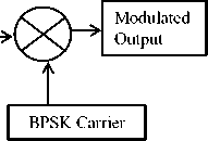
A. Conventional BPSK Transmitter
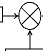
The Binary data is enforced to Encoder block. The data is converted to NRZ format. The carrier sine wave generated by local oscillator is applied to the multiplier block with the NRZ output to originate the BPSK Modulated output as depicted in Fig. 1.
Modulated Output
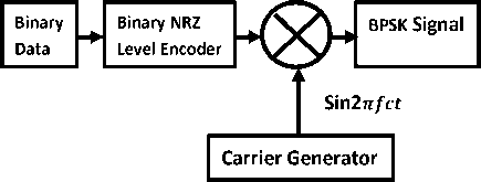
Fig.1. Conventional BPSK Modulator.
-
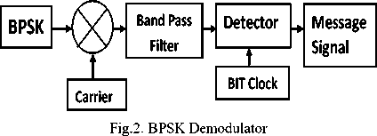
B. Conventional BPSK Receiver
A conventional BPSK demodulator is indicated in Fig.2. The BPSK demodulator comprises of mixer, band pass filter and detector. The modulated BPSK signal is multiplied on the carrier signal originated by the local oscillator. The signal is band limited and enforced to the detector. A detector makes a conclusion on each bit based on a threshold to create the Message Signal.
-
IV. Proposed BPSK Modulator with Booth ALgorithm
The BPSK Modulator with Booth algorithm is as shown below in Fig. 3. The conventional multiplier is replaced with the Booth multiplier. The encoder output and sine data are enforced to the Booth Multiplier. The rendered output results with the BPSK signal. The Power, Area and Gate requirement report of Proposed BPSK Modulator with Booth algorithm in 180nm, 90nm and 45nm CMOS technology is interpreted in Table 1.
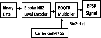
Fig.3. BPSK Modulator with Booth Multiplier.
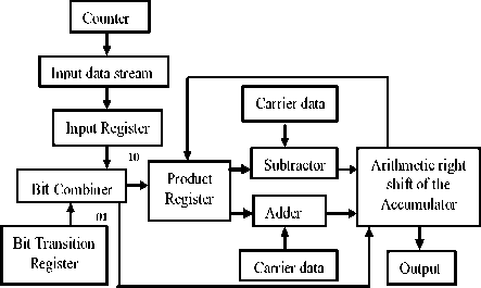
The implementation of BPSK using Booth multiplier is as pictured below in Fig. 4. If the input bit stream is 10, the phase data is subtracted from the product register and arithmetic right shift is executed, if the input bit stream is 01, the phase data is appended to the product register and arithmetic right shift is carried out. If the input bit stream is 00 or 11, directly the arithmetic right shift is attained on the data.
00 or 11
Fig.4. BPSK Modulator with Booth Multiplier.
-
V. BPSK Modulator with Iterative Algorithm
An iterative algorithm is employed to yield digital sine and cosine waves. The block diagram below in “Fig. 5,” designates the implementation of iterative algorithm.
Sine and Cosine values are calculated using this knowledge and computed values are placed in sine_reg and cos_reg respectively, as shown in the flowchart below in Fig. 6. The generated sine and cosine values are allowed to the modulator block. The information data stream is procreated with the carrier data to bring forth the BPSK.
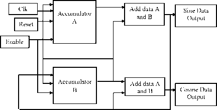
Fig.5. Block diagram depicts the Implementation of iterative algorithm.
In first step, clock, reset and enable pins are initialized, sine and cosine registers are affirmed with two integers m and n. If the clock and reset are enabled, then sine and cosine values are computed. If clock and reset are disabled, then sine and cosine registers are stored with the initial values.
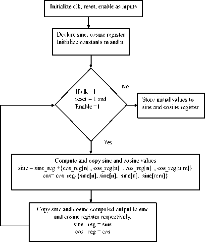
Fig.6. Flow chart shows sine and cosine generation using proposed Iterative algorithm-2.
-
VI. Proposed BPSK Modulator-3
The proposed BPSK Modulator-3 is revealed below in Fig 7. It is the simplified block diagram. It comprises of selector and control block. Initially the digital carrier data generated from the above blocks are stored in memory, Later the carrier phase data is picked out accordingly with the input data.
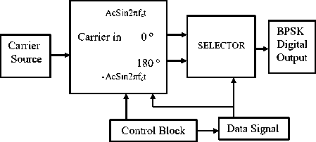
Fig.7. Proposed BPSK Modulator-3.
-
VII. Results
-
A. Conventional BPSK Modulator
The results of conventional BPSK modulator are represented in Table 1, below. The Table details about Leakage Power and Dynamic power. The total power is the addition of dynamic and leakage Power. The total power in nW and area in um2 is comprised in 180nm, 90nm and 45nm CMOS technology. The power consumption is reported as 174059 nW, 52432 nW and 12083nW in 180nm, 90nm and 45nm CMOS technology respectively. The area utilized is covered as 8968µm2, 2894µm2 and 692µm2 in 180nm, 90nm and 45nm respectively. The area and power requirement decreases with the technology.
Table 1. Power and Area Report of conventional BPSK Modulator
|
Technology |
Cells |
Leakage Power(nW) |
Dynamic Power(nW) |
Total Power (nW) |
Total Area µm2 |
|
180nm |
477 |
219.784 |
173840.05 |
174059 |
8968 |
|
90nm |
476 |
11719.097 |
40713.10 |
52432 |
2894 |
|
45nm |
448 |
354.211 |
11729.458 |
12083 |
692 |
B. BPSK Modulator with Booth Algorithm
The results of BPSK Modulator with Booth Algorithm in 180nm, 90nm and 45nm are detailed in Table 2. The power consumption is accounted as 86165.7nW, 22260.2nW and 3848.8nW in 180nm, 90nm and 45nm CMOS technology respectively. The area utilized is described as 1869µm2, 584µm2 and 146 µm2 in 180nm, 90nm and 45nm respectively.
Table 2. Power and Area Report of BPSK Modulator with Booth Algorithm
|
Technology |
Cells |
Leakage Power (nW) |
Dynamic Power (nW) |
Total Power (nW) |
Total Area µm2 |
|
180nm |
120 |
53 |
86112.6 |
86165.7 |
1869 |
|
90nm |
134 |
2222.7 |
20037.5 |
22260.2 |
584 |
|
45nm |
139 |
80.5 |
3765.2 |
3845.8 |
146 |
C. BPSK Modulator using Iterative Algorithm
The results of BPSK Modulator using Iterative Algorithm are covered in Table 3 below. The total power in nW and area in µm2 in 180nm, 90nm and 45nm CMOS technology is pointed below in Table. 3. The total power consumed by using this approach is 231214.0nW, 58868.6nW and 8033.8nW respectively in 180nm, 90nm and 45nm CMOS technology. The total area utilized using this method is 4847µm2, 1505 µm2 and 432µm2 in 180nm, 90nm and 45nm CMOS technology respectively.
Table 3. Power and Area Report of BPSK Modulator with Iterative algorithm
|
Technology |
Cells |
Leakage Power (nW) |
Dynamic Power (nW) |
Total Power (nW) |
Total Area µm2 |
|
180nm |
151 |
149.8 |
231064.6 |
231214.0 |
4847 |
|
90nm |
139 |
8058.0 |
50810.5 |
58868.6 |
1505 |
|
45nm |
173 |
242.0 |
7791.8 |
8033.8 |
432 |
D. Proposed BPSK Modulator-3
Table 4. Power and Area Report BPSK Modulator with Proposed Algorithm-3
|
Technology |
Cells |
Leakage Power (nW) |
Dynamic Power (nW) |
Total Power (nW) |
Total Area µm2 |
|
180nm |
7 |
6.2 |
4882 |
4888.3 |
183 |
|
90nm |
8 |
301.9 |
1200 |
1502.0 |
57 |
|
45nm |
9 |
9.3 |
329 |
338.3 |
16 |
The power consumption and area utilization of BPSK modulator with projected architecture-3 is elaborated in Table 4. The total power consumed using this approach in
180nm, 90nm and 45nm CMOS technology respectively as 488.3nW, 1502nW and 383.3nW. The total area utilized using this approach in 180nm, 90nm and 45nm technology is 183µm2, 57µm2 and 16µm2 respectively.
-
VIII. Comparison and Analysis
The results obtained by each method are tabulated and compared. The following parameters of proposed approaches are compared with the conventional method.
-
1. Device utilization summary.
-
2. Power Consumption Report
-
3. Area Utilization Report
-
A. Device utilization Summary
The device utilized (LUTs and slices) by suggested approaches are compared with the conventional method. As elaborated in Table 5, the conventional method uses 98 LUTs and 57 slices. The proposed approaches use minimum LUTs and slices than the conventional method. BPSK Modulator with Booth algorithm uses 74 LUTs and 39 slices. The BPSK Modulator using iterative algorithm uses 57 LUTs and 33 slices. Proposed BPSK Modulator-3 uses one-4 inputs LUT and 1-slice. The last method utilizes minimum logic blocks. The Table 5 is pictured in Fig.8, below with bar graph.
Table 5. Device utilization Summary of Conventional and proposed BPSK modulators
|
Logic Utilization |
Convention al BPSK Modulator |
Proposed BPSK Modulator with Booth algorithm |
BPSK Modulator using Iterative algorithm |
Proposed BPSK Modulator -3 |
|
slides |
57 |
39 |
33 |
1 |
|
Slice Flip Flops |
48 |
40 |
||
|
4 input LUTs |
98 |
74 |
57 |
1 |
|
Number of IOs |
20 |
25 |
28 |
37 |
|
bonded IOBs |
20 |
25 |
28 |
37 |
|
IOB Flip Flops |
1 |
3 |
||
|
GCLKs |
1 |
1 |
1 |
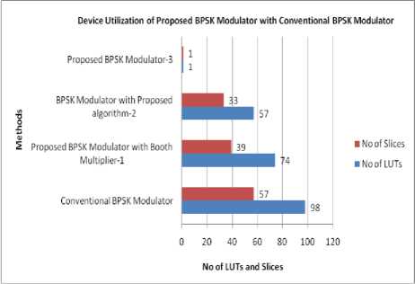
Fig.8. Device utilization summary.
B. Power Consumption Report
Table 6. Power comparison of conventional BPSK modulator with proposed BPSK modulator in 180nm, 90nm and 45nm technology
|
BPSK |
Conventiona l BPSK Modulator Power (nW) |
Proposed BPSK Modulator with Booth algorithm Power(nW) |
BPSK Modulator using Iterative algorithm Power(nW) |
Proposed BPSK Modulator-3 Power(nW) |
|
180nm |
174059.836 |
86165.696 |
231214.421 |
4888.261 |
|
90nm |
52432.198 |
22260.198 |
58868.566 |
1502.034 |
|
45nm |
12083.669 |
3845.788 |
8033.803 |
338.383 |
The power comparison of conventional BPSK modulator with proposed BPSK modulator in 180nm, 90nm and 45nm CMOS technology is rendered in Table 6. The power consumption is minimum in suggested BPSK modulators in comparing with the conventional BPSK modulator.
The power consumed by BPSK modulators is pictured in bar graph below in Fig. 9. The power consumed in conventional BPSK method is 174059.836 nW, 52432.198nW and 12083.669nW in 180nm, 90nm and 45nm CMOS technology respectively. The power consumed by BPSK Modulator with Booth algorithm is 86165.696nW 22260.198nW and 3845.788nW in 180nm, 90nm and 45nm respectively. The power consumed by BPSK Modulator with Iterative algorithm is 231214.421nW, 58868.566nW and 8033.803nW in
180nm, 90nm and 45nm technology respectively. Finally the power consumed by proposed BPSK Modulator-3 is 4888.261nW, 1502.034nW and 338.383nW in 180nm, 90nm and 45nm technology respectively. As shown in bar graph the power consumed by proposed Iterative algorithm is higher than the conventional BPSK Modulator. The other two proposed approaches consume minimum power than the conventional BPSK Modulator.
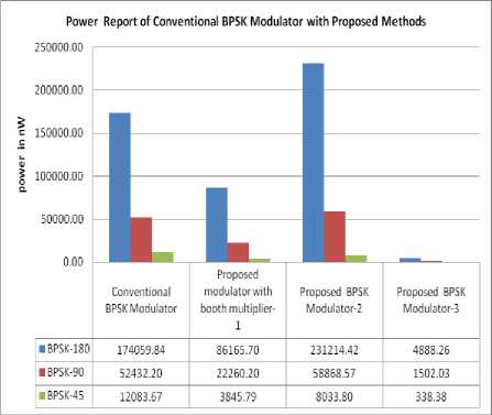
Fig.9. Power consumption report of conventional modulator with other proposed modulators.
-
C. Area Utilization Report
The conventional BPSK utilizes more area than the proposed BPSK modulators. Comparatively the BPSK modulator-3 utilizes minimum area than the other modulators. The area utilized by conventional BPSK Modulator is 8968µm2, 2878µm2 and 692µm2.
The proposed BPSK Modulator with Booth algorithm utilizes 1869µm2, 584µm2 and 146µm2. The BPSK modulator using Iterative algorithm utilizes 4847 µm2, 1505 µm2 and 432 µm2. The area employed by proposed BPSK modulator-3 is 183 µm2, 57 µm2 and 16 µm2 as depicted in Table 7. The synthesis carried out in 180nm, 90nm and 45nm CMOS technology respectively.
Table 7. Area Report of BPSK Modulator with Proposed Algorithm-2
|
BPSK |
Convention al BPSK Modulator Area µm2 |
Proposed BPSK Modulator with Booth algorithm Area µm2 |
BPSK Modulator Using Iterative algorithm Area µm2 |
Proposed BPSK Modulator-3 Area µm2 |
|
180nm |
8968 |
1869 |
4847 |
183 |
|
90nm |
2878 |
584 |
1505 |
57 |
|
45nm |
692 |
146 |
432 |
16 |
The Table 7 is pictured in bar graph below in Fig. 10. The proposed BPSK modulator using Iterative algorithm utilizes maximum area than the other proposed methods.
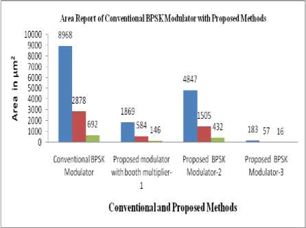
Fig.10. Area utilization report of conventional modulator with other proposed modulators.
-
IX. BPSK Modulator with AWGN Channel
The information data is transmitted over AWGN channel. The data is toned using BPSK modulator and transmitted over AWGN channel and extracted by BPSK demodulator as shown in Fig.11. The BER (Bit Error Rate) analysis for various values of Eb/No is carried out and results are indicated in Table 8, below.
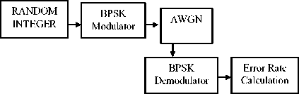
Fig.11. BER Analysis of BPSK Modulator over AWGN channel.
Table 8. Eb/No. Vs. Bit Error Rate Analysis.
|
Sl.No |
Eb/N0 |
BER |
|
1 |
0 |
0.09524 |
|
2 |
2 |
0 |
|
3 |
5 |
0 |
|
4 |
10 |
0 |
|
5 |
30 |
0 |
The Eb/No Versus Bit Error Rate analysis is carried out over AWGN channel using BPSK modulator and demodulator is indicated in Table 8, as the Eb/No step-ups, bit error rate diminishes.
As depicted below in Fig. 12. When Eb/No is 0dB, the error rate is 0.09524, when Eb/No increases from 0dB to 30dB, in steps of 5dB. The error rate minimizes.
BER Analysis of BPSK over AWGN Channel
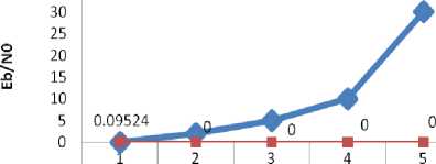
|
-♦-Eb/NO |
0 |
2 |
5 |
10 |
30 |
|
-■-BER |
0.09524 |
0 |
0 |
0 |
0 |
Fig.12. BPSK Modulator over AWGN Channel
-
X. Implementation of Digital Costas Loop
A Costas loop is a phase locked loop based circuit, which is used for carrier frequency recovery from suppressed carrier modulation signals. The main disadvantage of BPSK is that there will be phase errors in the received signal at the receiver end. To check the effective working of the receiver, a transmitter is designed. The design of the transmitter includes capturing an audio signal, sampling it and converting it into a digital signal, encoding it into a PN-sequence and modulating it using BPSK modulation technique. The transmitter section is depicted below in Fig. 13.

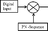
Fig.13. BPSK Transmitter with PN-Sequence.
At the receiver end, the BPSK signal received is demodulated as revealed in the Fig. 14, below.
Oscillator (NCO). The primary loop is I arm, which uses the NCO as in a Phase Locked Loop (PLL) and the second, Q arm uses a 90 degree tilted NCO signal. I and Q combiner outputs are filtered by single pole Butterworth low pass filter. I and Q arm channel outputs are multiplied together and the result is scaled and filtered to produce the loop error. This loop error is used to control the NCO. The loop error should settle to a value when the loop is locked. A negative loop error decreases the NCO increment resulting in a lower NCO frequency and a positive loop error increases the NCO increment resulting in a higher NCO frequency. The architectural level block diagram is as shown in the Fig. 15, below.
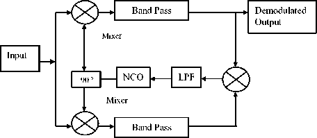
Fig.15. Architectural level block diagram of Costas loop.
-
XI. Simulation Results
The BPSK modulated signal is projected in Fig. 16. When the information bit is binary 0, the phase of the carrier is not varying. When the information bit is 1 the phase reversal is 180 degree. The phase modulated BPSK signal is generated.
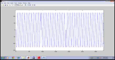
Fig.16. BPSK Modulated signal.
Fig.17. Below shows recovered message signal after demodulation.

Modulated Signal
^ Costas Loop
PN -Sequence
^ Output
Fig.14. BPSK Receiver with Costas Loop.
Costas loop involves two parallel crossing loops working together from the same Numerically-Controlled
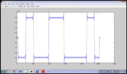
Fig.17. Message signal after demodulation.
The receiver can easily detect the message signal, whenever there is a change in the phase. The BPSK modulated message signal, the demodulated and filtered output is depicted in Fig. 18.
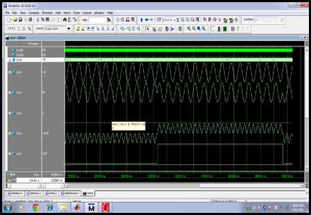
Fig.18. BPSK modulated message signal, the demodulated and filtered output.
-
XII. Conclusion
In this paper, new approaches for BPSK modulators are suggested. The area utilized and power consumed by new BPSK modulator architectural designs are compared with the existing conventional BPSK modulator and revealed that BPSK modulator using Booth Multiplier and proposed BPSK Modulator-3 consumes minimum power than the conventional BPSK method. The area and device utilization in proposed approaches is reduced in comparison with the conventional method. The simulation and synthesis is carried by using CADENCE tool. The work is carried out in 180nm, 90nm and 45nm CMOS technologies. The results are tabulated and compared and proved that the new approaches are efficient than the conventional technique in terms of power and area.
Acknowledgment
I wholeheartedly thank my college JSS Academy of technical education for providing me a lab facility to carry out this work.
References Low power and area optimized architectures for BPSK modulator
- U. Raza, P. Kulkarni, and M. Sooriyabandara, “Low Power Wide Area Networks: An Overview,” IEEE Communications Surveys Tutorials, vol. PP, no. 99, pp. 1–1, 2017.
- Rasoul Moradi, Ebrahim Farshidi Mohammad Soroosh, A low power passive-active ΔΣ modulator with high-resolution employing an integrator with open-loop unity-gain buffer”, Department of Electrical, Faculty of Engineering, Shahid Chamran University of Ahvaz, Ahvaz, Iran, sep 2018.
- H. P. Enterprise, “Low Power Wide Area (LPWA) Networks Play an Important Role in Connecting a Range of Devices,” Business white paper, November 2016.
- M. R. Palattella, M. Dohler, A. Grieco, G. Rizzo, J. Torsner, T. Engel, and L. Ladid, “Internet of Things in the 5G Era: Enablers, Architecture, and Business Models,” IEEE Journal on Selected Areas in Communications, vol. 34, no. 3, pp. 510–527, March 2016.
- Y. Roth, J.-B. Dor´e, L. Ros, and V. Berg, “Turbo-FSK, a Physical Layer for Low-Power Wide-Area Networks: Analysis and Optimization,” Elsevier Comptes Rendus Physique, vol. 18, no. 2, pp. 178 – 188, 2017.
- “LTE Evolved Universal Terrestrial Radio Access (E-UTRA): Physical Channels and Modulation,” 3GPP TS 36.211, V13.2.0, Release 13, Aug 2016.
- Y. Roth, “The Physical Layer for Low Power Wide Area Networks: A Study of Combined Modulation and Coding Associated with an Iterative Receiver,” PhD Thesis, University Grenoble Alpes, Jul. 2017.
- Y. Roth, J.-B. Dor´e, L. Ros, and V. Berg, “5G Contender Waveforms for Low Power Wide Area Networks in a 4G OFDM Framework,” in 2018 25th International Conference on Telecommunications (ICT) (ICT 2018), Saint Malo, France, Jun. 2018.
- Azad Mahmoudi, PooyaTorkzadeh, Massoud Dousti, “A study of analog decision feedback equalization for ADC-Based serial link receivers”, Department of Electrical and Computer Engineering, Science and Research Branch, Islamic Azad University, Tehran, Iran, Sept. 2018.
- Yoann Roth, Jean-Baptiste Doré, Laurent Ros, “Coplanar Turbo-FSK: A Flexible and Power Efficient Modulation for the Internet-of-Things”, Wireless Communications and Mobile Computing, August 2018.
- Y. E. Wang, X. Lin, A. Adhikary et al., “A Primer on 3GPP Narrowband Internet of Things,” IEEE Communications Magazine, vol. 55, no. 3, pp. 117–123, 2017.
- Y. Roth, J.-B. Doré, L. Ros, and V. Berg, “EXIT chart optimization of turbo-FSK: application to low power wide area networks,” in Proceedings of the 9th International Symposium on Turbo Codes Iterative Information Processing (ISTC '16), Brest, France, September 2016.
- M. R. Palattella, M. Dohler, A. Grieco et al., “Internet of things in the 5G Era: enablers, architecture, and business models,” IEEE Journal on Selected Areas in Communications, vol. 34, no. 3, pp. 510–527, 2016.
- Jinting Wang, Linjie Zhou, Haike Zhu, Qianqian Wu, Rui Yang, Lei Liu, Tao Wang, and Jianping Chen, “Silicon high-speed BPSK modulator: design and optimization”, Asia Communications and Photonics Conference 2014, OSA Technical Digest Optical Society of America, 2014.
- T. Rebbeck, M. Mackenzie, and N. Afonso, Low-Powered Wireless Solutions Have the Potential to Increase the M2M Market by Over 3 Billion Connections, Analysis Mason, 2014
- Asaraf Mohamed Moubark, Mohd Alauddin Mohd Ali,” FPGA implementation of low power digital QPSK modulator using Verilog HDL”,Journal of Applied Sciences, pp.385-392,ISSN 1812-5654, 2013.
- Hazrat Ali, Xianwei Zhou, Khalid Iqbal,”FPGA Architecture for OFDM, Software Defined Radio”, IEEE Journal, 2013.
- Fanxin Zeng, Xiaoping Zeng, Zhenyu Zhang and Guixin Xuan, “New constructions of 16-QAM periodic complementary sequences” IEEE communications, letters, Vol. 16, no.12, pp 2040-2043, December 2012.
- Masud, A., Samsuzzaman, M., Rahman, M. A., “Bit Error Rate Performance Analysis on Modulation Techniques of Wideband Code Division Multiple Access” Journal of Telecommunications, Vol 1, Issue 2, 2010.
- Wenmiao Song, Jingying Zhang, Qiongqiong Yao, “Design And Implement Of BPSK Modulator And Demodulator Based On Modern DSP Technology,” IEEE International Symposium. pp. 1135-1137, 2009.
- Y. Byungwook, H. L. Kyu and L. Chungyong, “Implementation of IEEE 802.16e MIMO-OFDMA Systems with K-BEST Lattice Decoding Algorithm”, International Conference on Consumer Electronics. Las Vegas, NV, USA, 2007.
- Charles U. Ndujiuba, Oluyinka Oni, Augustus E. Ibhaze, “Comparative Analysis of Digital Modulation Techniques in LTE 4G Systems,” Journal of Wireless Networking and Communications pp. 60-66, 2015.
