Methods used to develop the light emitting nanostructures with InGaAs/GaAs quantum wells

Author: Saeid S.
Journal: Физика волновых процессов и радиотехнические системы @journal-pwp
Article in issue: 1 т.20, 2017.
Free access
Light-emitting diodes based on InGaAs/GaAs quantum wells (QW) were fabricated and investigated. Cover layers of GaAs (15, 25, 35 nm) were deposited by high temperature (630 ˚C) epitaxy. Ferromagnetic Co metal layer was deposited by 60 ˚C and 90 ˚C and used as a spin injector. Incorporation of a tunnel-thin barrier of Al2O3 dielectric layer between the ferromagnet and the semiconductor cover layer leads to reduce the influence Co on the luminescence intensity, which indicates the reduction of penetration of impurity and defects into active region (QW). The experimental results demonstrate that manipulating of the cover-layer thickness and of the metal-film-deposition temperature improve performance and efficiency of spin injection light-emitting diodes.
Сpolarization, spin injector, tunnel-thin barrier, spin-polarized charge carriers, diffusion penetration, nanostructure, quantum wells
Short address: https://sciup.org/140255990
IDR: 140255990
Text of the scientific article Methods used to develop the light emitting nanostructures with InGaAs/GaAs quantum wells
It is possible to use the spin degree of freedom in the process of transfer and conservation of data and in the information processing. It allows developing a new type of smaller-sized devices with ability to transfer larger amount of information, to accelerate information processing and to reduce power consumption [1].
One of the examples of spintronic devices is a spin injection light-emitting diode based on InGaAs/GaAs quantum wells (QWs) and on Co ferromagnetic metal layer as an injector. The diode is considered as a source of circularly polarized light and as a promising device for data encoding and encryption [2].
Ferromagnetic metal contacts play a role of the injector for the spin-polarized charge carriers, which recombine with the opposite-sign carriers within the QW and thus it results in the circularly polarized electroluminescence. Emission of spin carriers in the spintronic devices is performed by the injection of spin-polarized charge carriers and by protection of their spin while the charge carriers transit the semiconductor cover layer. Therefore, a necessary condition for increasing of the spin injection effectiveness is reducing of the amount of defects in the interface between the metal and the semiconductor layers. It has been shown that an injecting charge carrier with significant spin polarization from a ferromagnetic metal into a semiconductor is possible through an injection process that is itself spin dependent [3]. Tunneling through a potential barrier can provide spin injection without losing spin polarization.
1. Experimental
Semiconductor/metal structures with substrates of n-GaAs (001) were grown under atmospheric pressure of hydrogen using metalorganic chemical vapor deposition (MOCVD) [4] for the semiconductor part. For the tunnel barrier/ferromagnetic metal part they were grown in vacuum using electronbeam evaporation. The structures contain three quantum wells (QWs) with different contents of In x = 0.25, 0.20 and 0.15 which are located at different depths: 35, 75, and 115 nm from the surface for the first sample, 25, 65, and 105 nm for the second sample and 15, 55, and 105 nm for the third sample. We used substrates of n-GaAs (001), so that the circular polarization happens due to injection of spin-polarized holes [5] from the ferromagnetic contact. Deposition temperature of the metal layer is 60 and 90 ° C, thickness of the cover layer is 15, 25, 35 nm. Chemical etching was used to remove the Co layer .The data obtained in the investigation of the structure was confirmed on cross-sectional samples using transmission electron microscopy (JEM-2100F).
hu, eV
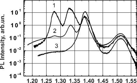
Fig. 1. The PL spectra of the structure with three quantum wells: 1 – initial sample; 2 – after deposition of Co at temperature of 60 ° C; 3 — after deposition of Co at temperature of 90 ° C
Electro-photoluminescence is measured at 77 K. Impurities and the distribution of components were an alyzed at the cross-section al structure with the help of Energy dispersive X-ray spectroscopy (EDS), integrated in the electron microscope. The photoluminescence (PL) was excited by He-Ne laser with power of 30 mW, and spectra were recorded at 77 K.
2. Results and discussion
Fig. 1 (curve 2 and 3) shows the photoluminescence (PL) spectra of the heterostructure after deposition of Co layer at temperatures of 60 ° C and 90 ° C respectively and its removing according to the method of chemical etching.
For comparison there given a spectrum of the original structure (Fig. 1, curve 1). PL peaks at 1.28, 1.34 and 1.39 eV correspond to the energies of the basic transitions in quantum wells (QW) with x = 0.25, 0.20 and 0.15.
Fig. 1 shows that as a result of deposition and removal of Co layer the PL peaks intensity of the QWs (with x = 0.25, 0.20), which are the first and the second from the surface, has decreased. For Co deposition temperature of 60 ° C the PL peak intensity, which is related to recombination in the QW1 has decreased by 100 times, and the PL peak intensity, which is related to recombination in the QW2 has decreased by 20 times. For Co deposition temperature of 90 ° C no photoluminescence at 1.28, 1.34 eV energies is recorded (with the exception of the background signal). Such a reduction of PL peaks intensity is attributed to an increase of concentration of defects resulting from Co deposition.
To analyze the defect formation we have carried out additional researches of Co and In
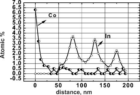
Fig. 2. Concentration profiles of the elements in the depth of structure with three quantum well and Co layer
hv, eV
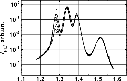
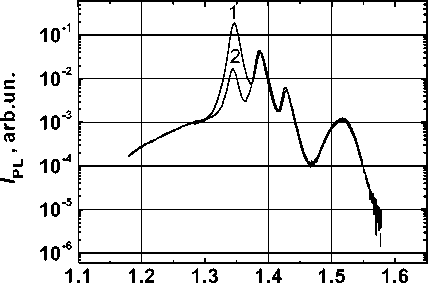
Fig. 3. The photoluminescence spectra of the structure with three QWs: 1 – initial sample; 2 – after deposition of Al2O3 (2 nm)/Со; 3 – after deposition of Al2O3 (1 nm)/Со concentration profiles by EDS analysis. According to the data of EDS analysis, the presence of Co atoms in the GaAs cover layer is registered, Co concentration decreases as the distance from the surface. In the area of the QW1 (near the surface) a signal of Co with the concentration which is slightly higher than the measurement error is registered. Co concentration in the area of QW2 and QW3 is equal 0 or is below the detection threshold.
According to the data shown in Fig. 1 and 2, it can be assumed that the PL quenching is due to the diffusion of Co atoms into QWs, which form nonradiative recombin ation centers. These centers suppress radiative recombin ation.
This assumption is confirmed by comparing the PL spectra of heterostructures with a Co layers deposited at temperature of 60 ° C and 90 ° C. A stronger quenching of the peaks from the QWs is observed for the structure with Co, deposited at 90 ° C than for a structure with Co deposited at 60 ° C. This may be due to an increase of concentration of diffusing Co that is a result of the increasing of deposition temperature.
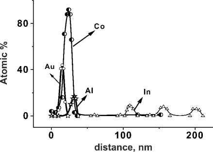
Fig. 4. Concentration profiles of the elements in the depth of structure with three quantum well and Al2O3 /Co layers
There was a proposal to form a thin (1-2 nm) intermediate Al2O3 layer between Co and GaAs to protect from Co atoms diffusion penetration into GaAs. Such layers serve as a diffusion barrier for Co atoms. In addition, for the selected range of thickness the Al2O3 layer is a tunnel - transparent one for charge carriers, another thickness of range ( > 2 nm) prevents current flow in the electroluminescent (EL) mode. The presence of the intermediate dielectric has a positive effect on the spin injection. Fig. 3 (curve 3 and 2) shows heterostructure PL spectra after deposition and removal of Co/ Al2O3 layer with 1 and 2 nm thickness respectively. From the Fig. 3 it is seen that as a result of formation of Co/ Al2O3 /GaAs structure the PL peaks’ intensity of the QW, which is the first from the surface, has decreased. For the heterostructure with Al2O3 layer with 1 nm thickness the intensity of the peak has decreased by 5 times. For the heterostructure with Al2O3 layer with 2 nm thickness the intensity of the peak has decreased by 2 times.
Comparing Fig. 1 and 3 it can be seen that the formation of a thin (1–2 nm) intermediate Al2O3 layer between Co and GaAs prevents quenching of the 2nd peak related with recombin ation in the QW2. The intensity of the 1st peak, relative to Co/GaAs structure, changes by deposing of Al2O3 by 20 and 50 times for 1 and 2 nm thickness of Al2O3 respectively.
Such an increase of PL peaks’ intensity is attributed to a decrease in the concentration of non-radiative recombination centers in the QWs region. EDS analysis data confirm the reducing of diffusion penetration of Co and the sharpness of “ferromagnet/semiconductor” interface (Fig. 4)
The Fig. 4 shows the concentration profiles of Co, In, Al and Au. It is seen that Co concentration
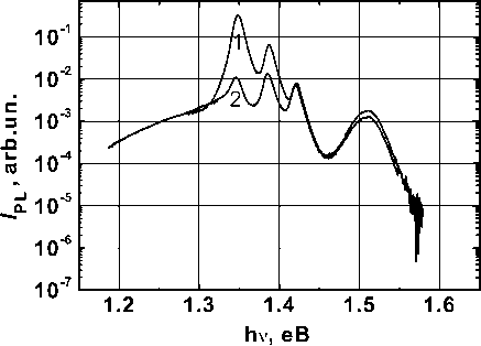
Fig. 5. The PL spectra of the structure with GaAs cover layer 15 nm: 1 – initial sample; 2 – after deposition of Al2O3 (1,2 nm)/ Co/ Au at temperature of 60 ° C
hv, eB
Fig. 6. The PL spectra of the structure with GaAs cover layer 25 nm: 1 – initial sample; 2 – after deposition of Al2O3 (1,2 nm)/ Co/ Au at temperature of 60 °C in GaAs is decreased compared to the case of Co/ GaAs (Fig. 2). In the region of the QWs 1, 2 and 3 Co signal is not registered. The obtained results are consistent with the assumption of slowing diffusion of atoms with Al2O3 layer.
From Fig. 5 it is seen that as a result of deposition and removal of Co the PL peaks’ intensity of the QWs, which are the first and the second from the surface, has decreased. For the heterostructure with GaAs cover layer, the thickness of which is 15 nm, the peak’s intensity associated with recombin ation in the QW1 has decreased by 28 times, and the PL peak’s intensity associated with recombin ation in the QW2 decreased by 4 times.
Fig. 6 shows that as a result of deposition and re-moval of Co the PL peak’s intensity of the QW1 has decreased. For the heterostructure with GaAs cover layer with 25 nm thickness the peak’s intensity associ-ated with recombin ation in the QW1 has decreased by 10 times.
Such a decrease of the PL peaks’ intensity is attributed to an increase of concentration of defects in the active region (QW) by applying Co.
Conclusions
It has been shown that the deposition of metal layers at high temperature leads to the acceleration of diffusion penetration of ferromagnetic metal atoms. In addition, decrease of Co deposition temperature, manipulation in the thickness of the cover layer and use of Al2O3 intermediate dielectric layer with different thicknesses reduces the amount of defects in the structure, thus the degree of polarization increases. Thickness of the cover layer is a diffusion barrier for active regions (QWs) and also it is a path for polarized carriers. In other words, thickness of the cover layer is a key factor to control both the amount of defects in the active region of the diode and the polarization of charged carriers.
References Methods used to develop the light emitting nanostructures with InGaAs/GaAs quantum wells
- Sarma S.D. Spintronics // Am. Sci. 2001. № 89. P. 516.
- Zutic I., Fabian J., Sarma S.D. Spintronics: Fundamentals and applications // Rev. Mod. Phys. 2004. № 76. P. 323-410.
- Fundamental obstacle for electrical spin injection from a ferromagnetic metal into a diffusive semiconductor / G. Schmidt [et al.] // Phys. Rev. B. 2000. № 62. R4790-R4793.
- Using laser sputtering to obtain semiconductor nanoheterostructure / B.N. Zvonkov [et al.] // J. Opt. Tech. 2008. № 75 (6). P. 389-393.
- Electrical spin injection in forward biased Schottky diodes based on InGaAs-GaAs quantum well heterostructures / N.V. Baidus [et al.] // Appl. Phys. Lett. 2006. V. 89. № 18. P. 181118.
