Multiband Dielectric Resonator Filter (MBDRF) with Defected Ground Structure (DGS) for Wireless Application
 with Defected Ground Structure (DGS) for Wireless Application")
Author: Md Rashid Mahmood, M.T Beg
Journal: International Journal of Intelligent Systems and Applications(IJISA) @ijisa
Article in issue: 9 vol.6, 2014.
Free access
In this paper a multiband dielectric resonator with array of defect at the ground plane is proposed. Filter is constructed by placing high-quality factor 〖TE〗_01δ mode dielectric resonators on the microstripline. The focus is on the design process includes choosing optimum geometry of a dielectric resonator so that high Q can be achieved. This is designed without compromising miniaturization and efficiency. It is observed that the integration of dielectric resonator with DGS may be merged to achieve wide band.Two band with 6 GHz low pass filter and 2 GHz band pass filter has been achieved. The filter which is proposed for microwave communication is expected to have better quality factor compared to lumped elements-based BPF. The used MBDRF have bandwidth of 6GHz and 2 GHz with dielectric constant of 60±1.
Multiband Filter, Dielectric Resonator Filter, DGS Filter, High Q Filter
Short address: https://sciup.org/15010602
IDR: 15010602
Text of the scientific article Multiband Dielectric Resonator Filter (MBDRF) with Defected Ground Structure (DGS) for Wireless Application
Published Online August 2014 in MECS
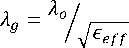
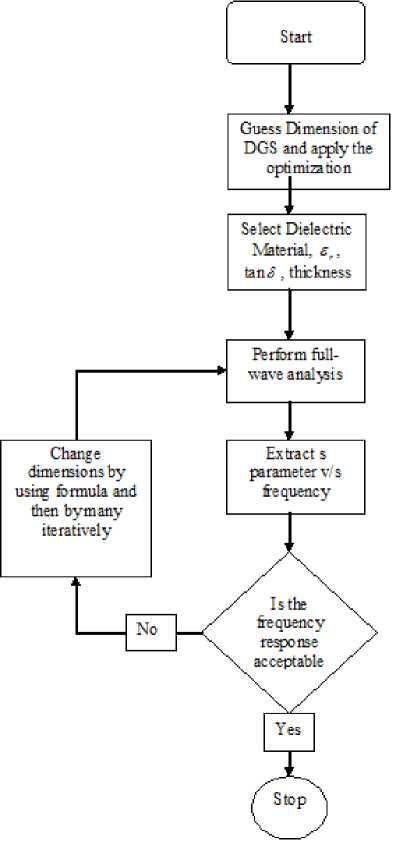
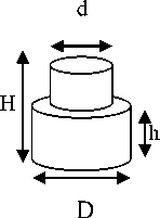
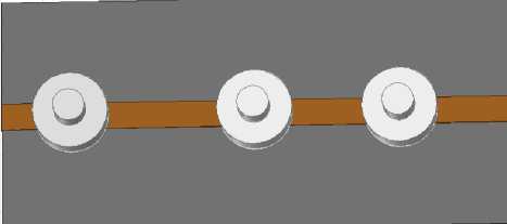
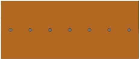
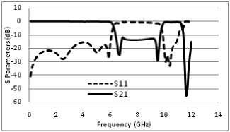
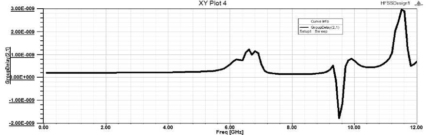
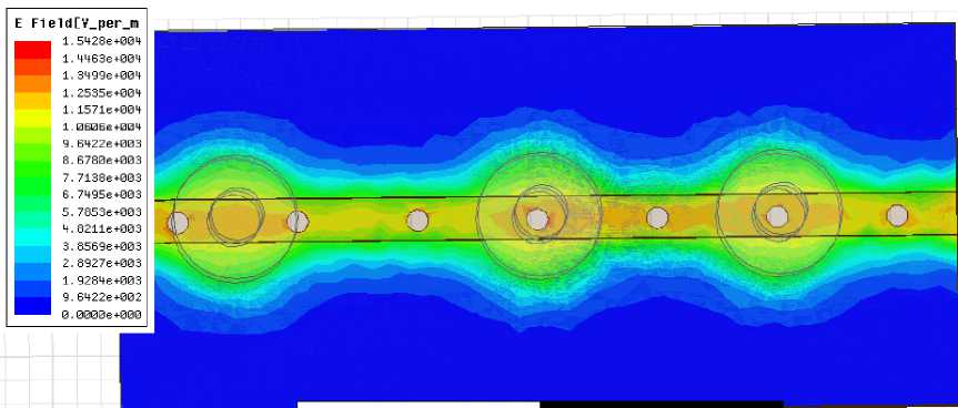
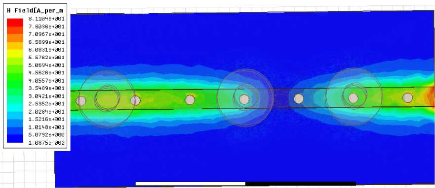
There has been tremendous progress in the development and deployment of wireless technologies in the last decade. The ubiquitous computing and communication environment is also provided by next generation wireless networks [1]. A wireless communication system demands a large number of basestation filters with not only an excellent in-band performance (i.e., low losses), but also a good out-ofband spurious performance. Dielectric-resonator filters are preferable for wireless base stations due to their superior characteristics of a high quality (Q) factor and miniaturization. However, cost reduction remains a key limiting factor for the wide spread use of dielectricresonator filters in base-station applications. There are increased demands for low-loss dielectric resonator filters that are compact and capable of being manufactured in a large quantity at a reasonable low cost. DRs are the basic building blocks in DR filters. Fields inside a resonator store energy at the resonant frequency where equal storage of electric and magnetic energy occurs. An advantage of DRs over corresponding metal wall cavities is they can be shaped to perturb the fields inside the evanescent cavity, whereas, it is impossible to shape a hollow cavity without inserting extra materials. Typically, DRs have a disc form that can be modified to include notches, chamfers and holes to control spurious modes and in multiple-order devices, these perturbations may address issues of inter-modal couplings. Three conventional shapes of DRs are rectangular, spherical and cylindrical, among the theoretically explored geometries, the cylindrical shape, L Therefore, radiation loss is minimal and the unloaded Q of the resonator is limited mainly by losses inside the dielectric body. Electric field losses occur as a result of the finite loss tangent (tan δ) of the dielectric material. If all of the electric energy of the resonant mode is stored inside the DR, and if no losses occur due to external fields, the unloaded Q will be given by Qu = 1⁄ tan5 (1) For all practical DR, there will always be some external loss due to radiation or dissipation in a surrounding metal shield. These losses tends to reduce Qu , while external stored electric energy tends to increase Qu for£ron the order of 100 or higher, these effects are small and Q = 1⁄ is a good approximation for the unloaded Q of a DR [3]. Size Fig. 1. Relative insertion loss and size of various RF resonators For all practical DR, there will always be some external loss due to radiation or dissipation in a surrounding metal shield. These losses tends to reduce Qu , while external stored electric energy tends to increase Qu for£ron the order of 100 or higher, these effects are small and Q = 1⁄ is a good approximation for the unloaded Q of a DR [2]. For the fundamental-mode resonance, the dimensions of a DR are on the order of one wavelength in the dielectric material. Since Ad = √ £r where Л^ is thewavelength in the dielectric, λ is the wavelength in air, and 8^ is the relative dielectric constant, the resonator dimensions are small compared to λ if E^ is large. Because the dimensions of an ordinary air-filled waveguide cavity are on the order of λ, a DR can be much smaller than a cavity resonator. The most practical configuration of the DR is usually a cylindrical disk whose length H is less than it’s diameter D. With this shape, the lowest-frequency resonant mode is the TEois mode, which has a circular electric field distribution. A drawback of the DR is that the resonant frequencies of the modes are close to each other. To make the DR practical for most applications, one of the goals of the resonator design is to separate the resonant frequency of the operating mode as far as possible from those of other modes. The DR aspect ratio (thickness/diameter) can also exercise some effect on tuning and Q, but a choice of H/D = 0.4 is recommended for both optimum Q and minimum interference of spurious modes for TEois mode operation [4]. Introducing a hole at the centre of the DR, i.e., ring resonator, can improve the separation between the TEoismode (fundamental mode) and higher-order modes [5]. The spurious characteristics are improved as a function of ring diameter. This property can be used to improve the spurious performance for dielectric loaded filters. The dielectric constant of a material is a parameter that reflects the capability of a material to confine a microwave. The higher this parameter means better in term of microwave signals confinement in the substrate. There is an inversely proportional between size and dielectric constant. A high dielectric constant is required to reduce circuit size of a device. The main difference lies in the fact that the wavelength in dielectric materials is divided by the square root of the dielectric constant E-p in a function of Where Ло is the free space wavelength at the resonant frequency. Moreover, unlike resonant cavities, the reactive power stored during resonance is not strictly confined inside the resonator. The leakage fields from the resonator can be used for coupling or adjusting the frequency. The wavelength inside the DR, guided wavelength ^y is also inversely proportional to the square root of the dielectric [6] The resonant frequency and radiation Q-factor can be varied even dielectric constant of the materials are fixed due to the dielectric resonators able to offer flexible dimensions.Dielectric resonators are being increasingly employed in a variety of microwave components and subsystems such as filters and oscillators. One of the most desirable resonator properties is simple tenability over a reasonably wide frequency band [7]. The usual approach is to provide some means of perturbing the fields surrounding the resonator, such as a tuning screw placed at a location of strong electric field or a tuning plunger that essentially varies the enclosure’s dimensions. Unfortunately, these approaches have two major limitations. First, they provide very narrow tenability ranges (if the unloaded Q’s are to be maintained at a high value), because the fields are usually concentrated within the dielectric material due to its high relative permittivity, and the effect of perturbing the weak external fields on the resonant frequency of the structure is very small. Second, if the tenability range is increased, the proximity of the conductors to the resonator causes severe degradation to the unloaded Q. In wireless LAN such as IEEE 802.1 communication systems, small size and high performance filters are needed to reduce the cost and improve the system performance. They can be designed in many different ways and by using different materials. Ceramic material with a high quality factor (Q×f) value (>10000) and a high permittivity provides a means to create small resonator structures such as coaxial structures that could be coupled to form comb-line band pass filters [8]. However, further miniaturization becomes more difficult for this filter. Planar filters with using high permittivity ceramic substrate provide good miniaturization ability. Therefore, there has been much research conducted on planar filters and their components. Since microstrip resonators are the basic components of a planar filter design, it is necessary to select proper resonator types used in a filter design [9]. The rectangular ring resonator can provide better performance such as narrow bandwidth in pass band and lower insertion loss when compare with other ones. A conventional rectangular ring microstrip resonator is too large to be used in the modern communication system. In this paper a dielectric resonator placed on the top of the strip of microstrip line, at the ground plane circular defect is etched. Microstrip line used in this paper is FR4 epoxy with dielectric constant 4.4. High Frequency Structure Simulator (HFSS) software is used for design and simulation. After tuning and optimization of the placing of DRs, we get the desired result. II. Design Methodoogy The size, location and shape of the dielectric affect the impedance matching of a microwave circuit. In this project three dielectric resonators were excited with a simple microstrip line in order to obtain the optimum coupling effect. A match combination of dielectric resonators and microwave circuit capable to generate an additional coupling effect that can be merged together to produce a wideband device as well as increasing the transmitting power and reduce the insertion loss. Holes are created at the ground plane which provides defected ground structure (DGS) so that it can reduce the harmonics and volume too. The stringent requirements of modern microwave communication systems are often met only by high performance and compact filtering structures. Several of such filters have been reported using generic structures called the defected-ground structures (DGS). Since DGS cells have inherently resonant properties, they have been used in filtering circuits to achieve narrow bandwidth, and to suppress these spurious pass bands. The DGS-resonators have several advantages such as compact size, low radiation loss. Therefore, the DGS-Filters are widely used in the design of filters, oscillators, and antennas. In MICs and MMICs designs, the circuit size has always been the center of attention due to circuit miniaturization and material cost reduction. For this propose, slow-wave structures such as metal-insulator-semiconductor (MIS) planar lines and capacitive or inductive loaded transmission lines have been widely examined [10], which are compatible with monolithic circuit technology. Also, in order to create the slow wave effect to reduce the circuit size as well as wide and deep stopbands to reject unwanted frequencies, many periodic structures including photonic bandgap (PBG) and defected ground structure (DGS) have been extensively investigated. In order to construct such structures in planar technology, these approaches require only partial etching of the ground plane or signal strip of a microstrip line or coplanar waveguide (CPW). In microstrip, due to etching of the ground plane, the dielectric substrate must be suspended so that the circuits cannot be located on a metal support to attain mechanic robustness and to make easy heat removal. The loaded planar structures on its signal strip are inappropriate for high power applications because of its great discontinuities and very thin line within the main signal path. On the other hand, the etched pattern on the signal strip is restricted to the dimension on the strip itself and excessive loss is generated because of the discontinuities created on the signal strip. MIS structures also are not suitable for applications at high frequencies. Therefore, the structuring of the ground plane may technologically be much easier and more suitable than processing of the signal strip for practical use in microwave applications. The quasi-lumped element based on the photonic-band gap (PBG) ground plane and the defected ground-plane structures (DGS) have been proposed to improve rejection in the stop band of a low-pass filter (LPF). However, the DGS has not been used to improve the stop band characteristics of the LPF. The researchers have commented that for the equal area of slot head, any shape of slot can be used. However, an equal area only ensures equal equivalent inductance and not the identical response of the DGS circuit elements [11]. A particular shape of the slot in a ground plane could also be more appropriate to design a complete circuit on the same substrate. The shape, size, and orientation of a slot can have an influence on performance of the filter and other neighboring circuits. Here we report a new DGS based band accept configuration in a microstrip line, by which we combined the band reject and band accept DGS configuration with microstrip to developed a compact seven pole low pass filter. Recently DGS have been gaining interest for their planer form and ease of fabrication. They are very useful in the design of LPF and BPF, since a few DGS can provide a cut-off frequencies and an attenuation pole without a need of periodic array as compared with EBG structure. The latter needs many units to build a filter. One advantage of employing DGS is that the fabrication cost can be reduced with a simultaneous improvement of the filter performance. Another advantage is that they can be easily modeled using simple RLC circuits, especially for microstrip line structures. Because of the excellent stop-band and slow-wave characteristics, the DGS have been applied widely to microstrip circuits such as filters, amplifiers and antennas. DGSs are realized by etching defects in the backside metallic ground plane under a microstrip line. A basic and widely used DGS cell is composed of two wide defected areas and a narrow connecting slot. A DGS-slot combination has a simple structure and can be modeled as a parallel LC resonator. Such a structure blocks the signal around its resonant frequency and may be used to introduce a wide stop band for low-pass and band-pass filters. Such filters have sharp transitions between the pass band and the stop band, low insertion loss in the pass band, wide stop band and high attenuation in the stop band [12-13]. This combination proficiently produces a low design profile. There is an inversely proportional between size and dielectric constant. Fig 2 shows, how the selection of DGS to be chosen for desired resonant frequency [14] Fig. 2. Flow chart of Conventional design and analysis method of DGS A high dielectric constant is required to reduce circuit size of a device. A significant miniaturization can be achieved, thus high-quality filters can be realized. The DRs used in this filter are cylindrical stair in shape, Geometry of resonators are shown in the Fig.2, which are in stair cylindrical in shape. Total length of microsrip line is 35mm; the centre position of first resonator is 10mm, second resonator at 17.5mm and third resonator at 30.2mm from left port respectively. Dielectric constant of resonator is 60. The unloaded Q is 3500. The seven holes are created at the ground plane which is 1mm in diameter. The resonant frequency is given by [9] /о = =( + 3.45) (2) √ Fig.3 shows the structure of resonator. Where r is radius and H is the height and £у is the dielectric constant of resonator. The dimensions of the DR specify its fundamental mode. H=3.5mm D=5.2mm h= 1.9mm d= 1.1mm Fig. 3. Geometry of dielectric resonator Among all these modes the TEois mode is the most interesting one because it is usually the dominant mode and it is simple to excite. The electric field is confined inside the resonator and is parallel to the boundaries but the magnetic field is perpendicular to the boundaries. Hence, in this mode the DR can be modeled as a magnetic moment vector aligning with the axis of the cylindrical resonator. To achieveTEoismode the height of the DR must be in between 35% to 65% of the diameter [15]. The lowest mode of the DR is set close to the lower end of the desired operating band as the starting point. Since dielectric permittivity values are fixed, the parameters diameter and height of DR used to determine the overall operating band of the filter. The placing between the resonators on the microstrip line used to tune the operating band and/or to achieve good impedance matching within a desired band. Following this method, a DR filter has been designed and optimized using HFSS simulator. Fig.4 shows the top view with resonator placed on microstrip line and Fig.5 shows the bottom view with circular DGS at the ground plane. Fig. 4. Top view of dielectric resonator filter Fig. 5. Bottom view of dielectric resonator filter Wideband filter can be designed using two or more DRs. All DRs are operating in a same principle. Each DR will resonate for a same mode but with different frequency such that the combination response is an additional result from the single response which able to increase the overall bandwidth. For example if DR1 has a normalized resonant frequency of and bandwidth of BW1, while DR2 has a normalized resonant frequency of and bandwidth of BW2, then the combination response could has a bandwidth BW that is larger than the sum of BW1 + BW2, if and are properly chosen. If the Q factors of the two resonators are approximately the same ( ≈ ≈ ) and if the return loss of thecombined response is equal to or better than 10 dB over the bandwidth BW, then the required values for the resonant frequencies of the individual DRs can be approximately equal to [9]: ≈(1- ) , ≈(1+ ) (3) Assuming the bandwidths of the two DRs are also similar ( ≈ ≈ , then the combined bandwidth is approximately BW = 3 by ignoring any mutual interaction as well as any loadingeffects of the feed, that could either increase or decrease the bandwidth response. When we vary the dimension of various parameter of Dielectric Resonator (DR) for optimization we realize that the resonance frequency f of filter depends on the physical dimensions of the DR. Using the tuning and optimization functions of 3-D simulator, a double band DR filter was obtained. The relationship between unloaded Quality factor, loaded Q and external Q is given by the relation. QL =& +Q Where QL is loaded Quality factor and Qe is external Quality factor. Coupling depends upon the mode of the resonator to be excited, and amount of coupling required. For fundamental TE mode of cylindrical dielectric resonator’s magnetic coupling is optimum solution as there is enough magnetic fields coming out of the resonator radially. Dielectric resonator size and distance between resonators define the internal coupling for resonators. Based on the transmission line equation, the coupling coefficient between a microstrip line and a dielectric resonator can be calculated [10] = = *∫ ( ) ( ) + (5) where is the resonant frequency, is the unloaded quality factor of the dielectric resonator, is the external quality factor, is the electric field along the microstrip transmission direction, W is the maximal magnetic energy of the dielectric resonator, and is the characteristic impedance of the microstrip line. Coupling coefficient between dielectric resonators could be calculated from the dipole moment in a distributed manner). The dipole moment is defined as follows () ( , , ) ∭ () ( , , ) where () is the dielectric constant, is the magnetic field along the z-axis direction, M is the total magnetic dipole moment of one dielectric resonator, and = ∭ .( ) (7) Where, R is the displacement vector, and E is the electric field. The coupling coefficient between two dielectric resonators can be written in terms of the dipole moment density as = ∑ ∭ ∭ ,(h (x,y ). (x,y,z ))(h (x ,y ). (x ,y,z )) exp(-τ (z -z ))- (8) where is the permeability, is the resonant frequency, W is the stored energy, m is the distributed magnetic dipole moment, h is the magnetic field of normal mode q, τ is the propagation constant of normal mode q, , v is the volume of the dielectric resonator at s and v is the volume of the dielectric resonator at s . Fig. 6. Frequency response of Dielectric Resonator filter Fig. 7. Group delay response of filter Fig. 8. E-field variations Fig. 9. H-field variations If the distribution of the electromagnetic fields is known, we can find the dimensions of the constitutive circuit elements from the formulae above. Transmission loss and insertion loss is shown in the Fig.6 with two pass band (low pass and band pass). A very minor group delay response shown in the Fig.7. In Fig.8 it is very clear that Electric field distribution confined near the resonator. Fig.9 shows the magnetic field distribution of the filter. Table 1 shows the return loss, transmission loss, group delay and bandwidth at both the resonating frequency. Table 1. Calculated value of various parameters. Result Parameters Return Loss -25dB at 6.5GHz -30dB at 9.5GHz -14dB at 8 GHz Transmission Loss -0.3dB at 6GHz -0.15dB at 9.5 GHz -0.35 dB at 8 GHz Group Delay ~0ns uniformly flat from 6 to 8 GHz Band Width (3dB) (9.7-6.2)= 3.5GHz = 44% IV. Conclusion The application of TEois mode DRs for microwave filters around 6 GHz and 10 GHz has been investigated. The choice of the DR is discussed in detail. Finally, a TEois mode DR filter with inductive direct coupling is simulated. The developed dual-band dielectric-resonator filters are compact in size while offering a much higher in comparison with microstrip dual-band filters. DGS reduce the harmonics as well as overall size of the filter. Here we successfully design a very compact size of dual band dielectric resonator filter for wireless application, Here we observe dual band dielectric resonant filter with resonant frequency 6 GHz (Low pass), 10.75 GHz (band pass) with stop band of 3.3GHz. The pass band of band pass filter is 2 GHz Multiband Dielectric Resonator Filter (MBDRF) with Defected Ground Structure (DGS) for Wireless Application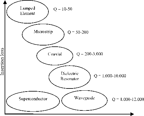
References Multiband Dielectric Resonator Filter (MBDRF) with Defected Ground Structure (DGS) for Wireless Application
- Kiran Ahuja, Brahmjit Singh, Rajesh Khanna, “Available Link Bandwidth Based Network Selection in Multi-access Networks”, I.J. Intelligent Systems and Applications, 2014, 03, 76-83
- R. Mansour,” High-Q tunable dielectric resonator filter”, IEEE microwave magazine, Vol 10, October 2009.
- Chi Wang and Kawthar A. Zaki, “Dielectric resonator and filter”, IEEE microwave magazine, October 2007.
- S.W. Chen and Z.A. Zaki,’Dielectric ring resonator loaded in waveguide and on substrate”, IEEE Trans Microwave Theory Tech, vol 39, p39, Dec 1991
- Y. Kobayashi and M. Minegishi,”Pricise design of a bandpass filter using high-Q dielectric resonator”, IEEE Trans Microwave Theory Tech, Vol. MTT-35 pp. 1156, Dec 1987.
- Mohd F. Ain, Ahmad A. Sulaiman, Zainal A. Ahmad, M.A. Othman, Ali Othman and Ihsan A. Zubir, “Ultra-Wideband Dielectric Resonator bandpass Filter”, European Journal of Scientific Research, ISSN 1450- 216X Vol.46 No.4 (2010), pp.503-509
- Xiaoming, X. and R. Sloan, “Distributed coupling model of the dielectric resonator to microstrip line." IEEE Microwave and Guided Wave Letters, vol. 9, pp. 348-350, Sept 1999.
- R. Zhang and R. R. Mansour, “Low-cost dielectric-resonator filters with improved spurious performance,” IEEE Trans. Microwave Theory Tech., vol. 55, pp. 2168–2175, Oct. 2007.
- Ahmad Munir and Javier Augustson Sitorus, “High Permittivity Circular Dielectric Resonator for 2-stage Narrowband Bandpass Filter”, 2012 7th International IEEE conference on Telecommunication System Services and Application.
- A.Petosa, Dielectric Resonator Antenna Handbook, Artech House, Bolton, 2007.
- Anand K. Verma, Adel B. Abdel-Rahman, Ahmed Boutejdar , & A.S. Omar “Control of Bandstop Response of Hi-Lo Microstrip Low Pass Filter Using slot in Ground Plane”IEEE, Transactions on MTT,Vol.52,No3,March 2004.
- J.S. Lim, C.S. Kim, Y.T. Lee, D. Ahn and S. Nam, “Design of Low Pass filters Using Defected Ground Structure and Compensated Microstrip Line,” IEE Electronics Letters, Vol. 38, No. 22, 24 October 2002, pp. 1357–1358
- Nemai Chandra Karmakar, , Sushim Mukul Roy, and Isaac Balbin, ” Quasi-Static Modeling of Defected Ground Structure”, IEEE Transaction of Microwave Theory and Techniques, VOL. 54, NO. 5, MAY 2006.
- L. H. Weng, Y. C. Guo, X. W. Shi, and X. Q. Chen, “An Overview of Defected Ground Structure”, Progress In Electromagnetics Research B, Vol. 7, 173–189, 2008.
- Md Rashid Mahmood, Prof M.T Beg, “TE01δ Mode Low Pass and Band Pass Dielectric Resonator Filter”, European Journal of Scientific Research, Vol 108, Issue 2.
