Nanotechnologies: a review of inventions and utility models. Part IV

Author: Ivanov L.A., Ishkov A.D., Pisarenko Zh.V., Wang Q., Prokopiev P.S.
Journal: Nanotechnologies in Construction: A Scientific Internet-Journal @nanobuild-en
Section: Review of nanotechnological inventions
Article in issue: 5 Vol.12, 2020.
Free access
The article provides an abstract review of patents. The results of creative activity of scientists, engineers and specialists, including inventions in the field of nanotechnology and nanomaterials, being implemented, allow achieving a significant effect in construction, housing and community services, and related sectors of the economy. For example, the invention “Heat-insulating material based on air gel” can be used to obtain heat-insulating materials for a wide range of applications. The required technical result, which consists in improving the thermal insulation properties of the material in a wide temperature range, increasing the absorbing properties of electromagnetic radiation in the IR spectrum, increasing the mechanical strength and flexibility, as well as reducing crumbling, is achieved in an air gel-based material containing a fibrous substrate with a density of 0.001–0.1 g/cm3, consisting of silica and/or glass and/or basalt fibers with a diameter of 0.1–5 microns, which is impregnated with an air gel obtained on the basis of silicon dioxide from alkoxysilane with the introduction of a gelling agent and followed by supercritical drying. The introduction of nanomaterials gives an additional reinforcing effect, which increases the mechanical strength of the final material and significantly reduces the crumbling of the air gel. The final material can be provided with an additional layer of fibrous substrate to increase its vibration resistance. This is especially true when using the proposed material for civil and industrial construction in seismically active zones, as well as in aircraft and rocketry. The specialists can also be interested in the following inventions in the area of nanotechnologies: nano-coating protection method for electrical connectors, preparation method of nanometric size metal oxide additives that reduce the temperature of sintering, raw material mixture for the manufacture of fine-grained polymer concrete (modified with microsilica), installation for the synthesis of carbon-containing nanomaterials, a method for producing silver nanoparticles, a method for producing nanocrystalline cubic tungsten carbide, a composition with carbon nanotubes for obtaining a carbon blank for high-density SiC/C/Si ceramics and a method for producing articles from SiC/C/Si ceramics, composite membrane for drying natural and technological gas mixtures based on graphene oxide intercalated with hydroxylated fullerene derivatives, compositions containing nanometric copper, carbon-ceramic fiber-reinforced composite material and a method for its production, a method for producing nanoparticles of aluminum oxide et al.
Nanotechnologies in construction, nano-coating, nanomaterial, carbon nanotubes, nanoparticles of aluminum oxide, nanometric copper
Short address: https://sciup.org/142226959
IDR: 142226959 | DOI: 10.15828/2075-8545-2020-12-5-275-284
Text of the scientific article Nanotechnologies: a review of inventions and utility models. Part IV
Advanced technologies impress people’s imagination demonstrating the latest achievements (materials, methods, systems, technologies, devices etc.) that dramatically change the world. This, first of all, concerns nanotechnological inventions designed by scientists, engineers and specialists from different countries.
REVIEW OF NANOTECHNOLOGICAL INVENTIONS
MAIN PART
Heat-insulating material based on air gel with the possibility of introducing nanomaterials into the final product (RU 2731479 C1)
The invention relates to technologies with the use of air gel and can be used to obtain heat-insulating materials for wide application [1]. The required technical result, which consists in improving the thermal insulation properties of the material in a wide temperature range, increasing the absorbing properties of electromagnetic radiation in the IR spectrum, increasing the mechanical strength and flexibility, as well as reducing crumbling, is achieved in an air gel-based material containing a fibrous substrate with a density of 0.001–0.1 g/cm3, consisting of silica and / or glass and / or basalt fibers with a diameter of 0.1–5 microns, which is impregnated with an air gel obtained on the basis of silicon dioxide from alkoxysilane with the introduction of a gelling agent and followed by supercritical drying.
The use of a fibrous substrate with a density of 0.001– 0.1 g/cm3, which consists of silica and or glass and/or basalt fibers of a given diameter of 0.1–5 microns and is characterized by a narrow distribution of fibers along the diameter. The fibrous substrate has a thermal conductivity of 0.020–0.025 W/(mK). The use of the specified fibrous substrate makes it possible to obtain a material based on an air gel with an extremely low thermal conductivity coefficient of 0.014–0.016 W/(mK). The use of fibers with a diameter of 0.1–5 microns with a narrow distribution along the diameter allows, on the one hand, to reduce its effect on the thermal conductivity of the final material, and on the other hand, to increase the efficiency of the reinforcing effect, and significantly reduce the crumbling of the air gel.
Possible introduction of nanomaterials into the final product: carbon nitrided nanoflakes, carbon nanofibers, carbon nanotubes, multilayer carbon nanotubes. These nanomaterials have the following properties: specific surface area 300–600 m2/g, bulk density 0.05–0.25 g/cm3, characteristic size 10–100 nm. Their introduction into the composition is carried out at the stage of obtaining a gel; various surfactants can be used to disperse nanomaterials.
The use of these materials gives the final material the following advantages:
– the absorption of electromagnetic radiation in the infrared range increases, due to which the thermal conductivity of the final material at high temperatures decreases;
– the introduction of nanomaterials of a given size makes it possible to correct the distribution of airgel pores in size, due to which the thermal conductivity of the airgel is advantageously reduced to values of 0.012– 0.014 W/(m•K);
– the use of nano materials gives an additional reinforcing effect, which increases the mechanical strength of the final material and significantly reduces the crumbling of the airgel.
The final material can be provided with an additional layer of fibrous substrate to increase its vibration resistance. This is especially true when using the proposed material for civil and industrial construction in seis-mically active zones, as well as in aircraft and rocket construction.
A method of manufacturing shaped products with a base of foamed polymers (RU 2731930 C1)
A method of manufacturing a profile product used as a load-bearing and self-supporting structure for door and window frames, transoms, and other structures requiring a combination of sufficient strength properties and low heat capacity is proposed [2]. A profile product is made by molding in a mold layer by layer, using a denser foamable or non-foamable layer as the shell of the product and a foamable base from at least one layer or with a combination of layers with different densities, which provides the required combination of strength and low heat capacity. Expandable polymer, composite materials, or non-foamable polymer and composite materials in combination with forming additives – microspheres are used as the base material. The strength characteristics of the product are ensured by the presence of modifying components introduced into the polymer media – nanoadditives, carbon microadditives, aluminosilicate microadditives, providing enhanced bonds with conglomerates of polymer macromolecules, as well as processing of polymer components by a high-frequency electromagnetic field immediately before their introduction into the mold.
The processing of components by a microwave field increases the bond energy of the monomers of the polymer composition during polymerization, both among themselves, and contributes to a significantly better distribution of micro- and nano-additives in the volume of the medium, which significantly increases the strength of the product, the density distribution in the mass, and significantly accelerates the polymerization process, providing the efficiency of the process and its industrial application. As a protective layer, it is permissible to use a non-foaming polymer composition applied by spraying onto the inner surface of the mold, any materials and decoration elements built into the mold before the start of pouring polymer media that form the base of the product, or additionally applied to the surface of the product. The product, obtained from polymers in this way, complies
REVIEW OF NANOTECHNOLOGICAL INVENTIONS with environmental standards, has a long service life, is resistant to weathering and ultraviolet light.
The structure of the technological process of the method for manufacturing a shaped product with a base of foamed polymers is shown in Fig. 1, which schematically shows:
-
1 – preparation of reagents - components of a polymer or polymer-composite mixture;
-
2 – adding modifying and non-modifying additives to the components of the mixture;
-
3 – component mixing device;
-
4 – a waveguide and a device for pumping the mixture for adjusting the time of processing the microwave with an electromagnetic field;
-
5 – mold;
-
6 – an internal overlay in the mold, which forms the external decorative coating of the product;
-
7 – an external fastening element integrated into the product, fixed in a mold;
-
8 – sprayer of polymer composition (medium).
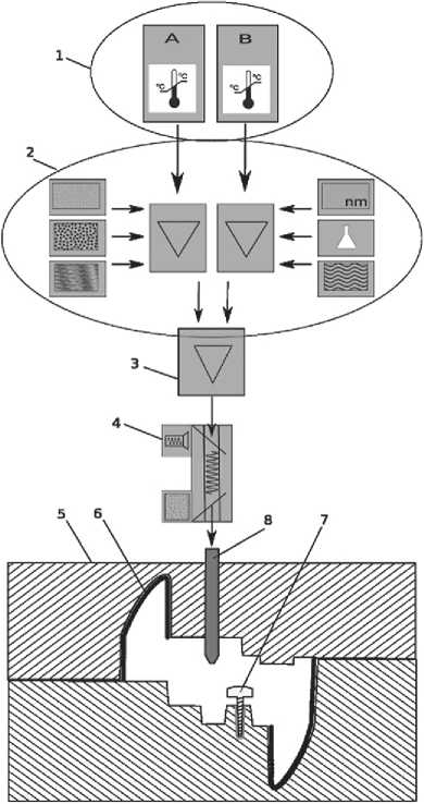
Fig. 1. The structure of the technological process of the method of manufacturing a profile product with a base of foamed polymers
Method for the synthesis of graphene-like layers in porous silicon structures (RU 2731278 C2)
The objective of the invention is to expand the scope of porous silicon structures with graphene-like layers located on the pore walls, by creating graphene-like layers on the outer and inner surfaces of both through and closed pores throughout the depth in a porous structure with an increased thickness of porous layers [3].
The problem is solved by the fact that in the known method for the synthesis of graphene-like layers in porous silicon structures, including the CVD process in ethanol vapor in an inert gas in a pressure drop mode in a quartz reactor, it is new that the temperature in the reactor is 800–1100оC, and To implement the differential pressure mode, the pressure is first raised from the operating value of 1•103 Pa to 5•104 Pa within a minute, then the pressure is released to the specified operating value within 5 seconds and the specified pressure drop mode is repeated after 9–11 minutes until graphene-like layers are obtained on the pore walls to a given depth.
If 11 minutes are exceeded, unwanted clogging of pore channels appears. At times less than 9 minutes, a discontinuity of the coating of the inner surface of the pore walls is observed. The most optimal process conditions are the temperature in the quartz reactor of 950оC and the repetition of the pressure drop mode after 10 minutes. The technical effect of the invention is the creation of graphene-like layers on the outer and inner surfaces of the pores, including closed , over the entire predetermined depth of the porous structure, reaching 148 microns in the prototypes.
The invention relates to the field of materials science and can be used to create molecular separation membranes, membranes for biological and medical applications, sensor and electronic devices, and also as electrodes for micro-fuel cells and other current sources.
Symmetrical four-pair cable with film-nanotube insulation of cores (RU 2731624 C1)
The invention relates to the field of electrical engineering and can be used in the construction of symmetrical communication cables for public networks and structured cable systems [4]. In a four-pair cable containing conductors in film-polymer insulation, twisted in pairs with different twisting steps into a common layer, with an outer polymer sheath, insulation of each core. The outer polymer shell of each core is made in the form of nanotubes of the same size over the entire cross section of each core, and some of the nanotubes are perforated. The outer film is in contact with the nanotube insulation of each core over the entire cross section; each core along the entire length of a balanced cable. The invention provides the creation of such a structure of a symmetri-
REVIEW OF NANOTECHNOLOGICAL INVENTIONS cal four-pair cable, which allows to reduce the relative dielectric constant of the insulation of the cable cores, to reduce the capacitance of pairs and, consequently, the dielectric losses and the capacitive component of the influence between pairs.
Fig. 2 shows the structure of a symmetrical four-pair cable with film-nanotube insulation of cores. The cable contains: symmetric pairs – 1, cores – 2, nanotube core insulation – 3, outer core insulation film – 4, in contact with nanotubular insulation, outer polymer cable sheath – 5. Thanks to the declared design, the relative dielectric constant of core insulation is significantly reduced due to nanotubes, inside which the relative dielectric constant is 1.0 (the relative dielectric constant of the air is 1). Depending on the number of nanotubes and perforated nanotubes, the relative dielectric constant can be changed over a fairly wide range, decreasing the insulation thickness and decreasing dielectric losses. The dielectric constant of the dielectric material is 2.3, taking into account the film-nanotube insulation when filling through holes of the nanotubes and contacting the veins in the volume of 100% of the entire volume of the conductor insulation, it is possible to obtain the relative dielectric constant of the entire conductor insulation equal to 1.9. As a result, the attenuation coefficient decreases due to a decrease in losses in the insulation of the conductors, the wave resistance and the capacitive component of the influence between the pairs, and due to the decrease in the thickness of the insulation and, therefore, the distance between the conductors in the pair, the inductance of the circuit also decreases.
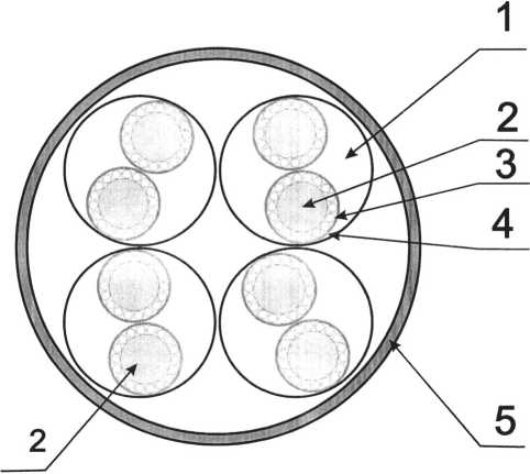
Fig. 2. Symmetrical four-pair cable with film-nanotube insulation of conductors
Method of alloying titanium dioxide of anatase allotropic modification with noble metal nanoparticles (RU 2731277 C1)
In connection with the constant development of the light industry, in particular, textile, food, paint production, as well as the emergence of new requirements for water quality, the problem of pollution of the water basin with organic dyes is acute. The proposed group of inventions relates to the field of chemistry, concerns the method of alloying powdered titanium dioxide nanoparticles of noble metals to create a highly efficient photocatalyst intended for photocatalytic reactions of oxidation of organic compounds under mild conditions, including azo dyes, phenol and its derivatives, which makes it possible to use photocatalysis reactions to purify water and air from trace organic pollutants by means of light irradiation (both ultraviolet and solar), and the creation of conditions for a safe and comfortable human habitation [5].
The technical result from the use of the proposed group of inventions is to simplify, reduce energy consumption when alloying the surface of titanium dioxide with nanoparticles of noble metals, increase the efficiency and uniformity of distribution of nanoparticles of noble metals on the surface of titanium dioxide.
The task is achieved by the fact that the method of doping titanium dioxide of anatase allotropic modification with noble metal nanoparticles includes preparing an aqueous solution of the salt form of chitosan, into which a precursor dopant of gold or silver nanoparticles is introduced, after which the system is intensively stirred and exposed to UV exposure to form noble metal nanoparticles at a temperature of 20–70оC, the formation of metal nanoparticles is monitored spectrophoto-metrically, and after reaching the maximum intensity of the plasmon resonance band of the nanoparticles, titanium dioxide of the anatase allotropic modification is introduced into the system with constant stirring, then an enzyme is introduced into the dispersion, the enzymatic decomposition of chitosan macromolecules is carried out at a temperature 35–40оC until complete degradation of chitosan; before the introduction of the enzyme into the system, an additional ultrasonic treatment of the dispersion is carried out with a frequency of up to 35 kHz; papain or pancreatin or amylase or glucoamylase or chitosan is used as an enzyme; the concentration of chitosan in the solution is 0.1–3% by weight, the concentration of titanium dioxide in the chitosan solution is 0.01–20% by weight of dry chitosan, precursors of noble metal nanoparticles – from 0.01 to 5% by weight of dry chitosan; after all the modified titanium dioxide has precipitated, the system is subjected to thermal treatment at a temperature of 70–100оC.
REVIEW OF NANOTECHNOLOGICAL INVENTIONS
Method of manufacturing bulk micro-sized structures from nanoparticles (RU 2730008 C1)
The invention relates to an additive 3D technology for the production of predominantly volumetric micro-sized structures from nanoparticles, which are used in electronics, photonics and other fields. The method of manufacturing bulk micro-sized structures from nanoparticles includes (Fig. 3) sintering nanoparticles on a substrate 5, obtaining an aerosol stream with nanoparticles in a transport gas flow in block 1, heating by a laser-optical device 6 in a block 8 for optimizing an aerosol with nanoparticles in a transport gas stream with ensuring the production of spherical nanoparticles, transporting the resulting flow through the outlet 10 of the unit 8 for optimizing the aerosol with nanoparticles to the head 3 with the nozzle 4 to focus it on the substrate 5, supplying the specified nozzle with a stream of aerosol with nanoparticles and at the same time a protective gas to ensure that the aerosol flow of nanoparticles is focused on the substrate and deposited nanoparticles from a focused aerosol flow onto the substrate [6]. The deposition and sintering of nanoparticles on the substrate are carried out in a protective gas atmosphere 13, which is created under the nozzle. The invention improves the flexibility and efficiency of the process control, to simplify the device in the implementation of the method by using one laser to heat the aerosol with nanoparticles in a transport gas flow to ensure the production of spherical nanoparticles and sintering of nanoparticles on a substrate.
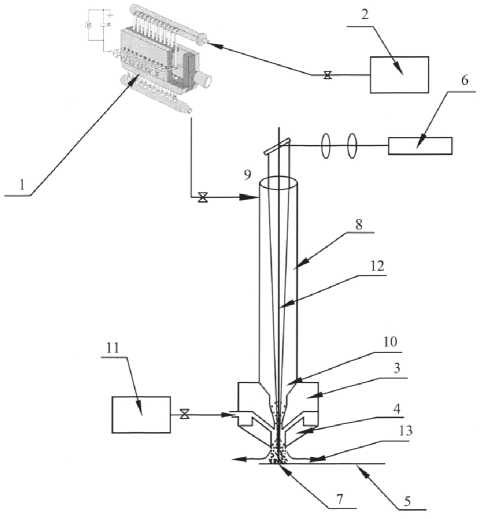
Fig. 3. A method of manufacturing bulk micro-sized structures from nanoparticles.
This technical solution makes it possible to produce bulk structures from nanoparticles. However, when using this technical solution, difficulties arise in changing the temperature when heating an aerosol with nanoparticles in a transport gas flow to ensure the production of spherical nanoparticles of the required size, since the heating elements used are inertial and a relatively long time is required, for example, to reduce the heating temperature. Also, two sources of heating are required – for sintering nanoparticles and for heating aerosol with nanoparticles in a transport gas flow.
The result, to achieve which this technical solution is directed, lies in the possibility of more flexible changes in the process parameters while reducing the amount of equipment used to implement the method.
Method for increasing the efficiency of metal hydride heat exchangers (RU 2729567 C1)
The invention relates to the field of heat power engineering and hydrogen energy, or rather, to heating or cooling devices (heat exchangers or heat pumps) based on reversible thermochemical cycles, which use the energy of low-potential heat sources of natural or man-made nature for operation [7]. In these devices, during thermochemical cycles, either the absorption of hydrogen by metals or alloys occurs with the formation of hydrides, which occurs with the release of heat, or the release of hydrogen during the decomposition of hydrides, accompanied by the absorption of heat. Hydrogen uptake occurs at a hydrogen pressure above the hydride formation pressure or at an external temperature below the dehydrogenation temperature, and hydrogen evolution occurs at a hydrogen pressure below the hydride decomposition pressure or at a temperature above the dehydrogenation temperature.
The novelty of the proposed method lies in the fact that dispersed elements, the material of which has a sufficiently low density and a sufficiently high coefficient of thermal diffusivity, are introduced into the composition of the metal hydride filling of the heat exchangers. This allows increasing the specific power of metal hydride heat exchangers and reduce the weight of devices, which is especially important for mobile applications of metal hydride technologies. Additionally, such additives can reduce the sintering capacity of the metal hydride backfill powders during hydrogen absorption-evolution cycles.
The proposed technical solution can also be used for other gas-phase applications of metal hydrides, such as hydrogen storage. The technical result is an increase in the specific power of metal hydride heat exchangers and a decrease in the weight of the device, as well as a decrease in the sintering capacity of the powders of the metal hydride backfill during hydrogen absorption-release cycles.
REVIEW OF NANOTECHNOLOGICAL INVENTIONS
Fiber-optic substance sensor (RU 2731036 C1)
The fiber-optic substance sensor belongs to the field of materials technology, materials science and analytical research and allows you to expand the field of application, while simplifying the design and increasing the sensitivity of the sensor, which contains (Fig. 4) a piece of fiber-optic cable (1), at one end of which there is an object microlens (2), and at its opposite end of the microlens (3), on the surface of the object microlens (2), a film (4) with the addition of carbon nanotubes is applied, while the sensor is installed on a plastic tag (5) to carry out the sampling process. The technical result obtained is provided by creating a signal of secondary Raman scattering, its amplification in the structure of carbon nanotubes and transmission of the amplified signal to the spectrum analyzer [8].
The fiber-optic sensor works as follows: The sensor is fixed on a plastic tag 5, which contains information about the coordinates and time of sampling. Then the plastic tag 5 with the sensor is placed in the slot of the portable spectrum analyzer, where a laser beam is directed to the object microlens 2, causing secondary Raman (Riemann) radiation from the particles of the substance captured by the film 4. This radiation, its spectral composition, is determined by the structure and composition of the molecule of the investigated substance, which allows the substance to be identified by the spectrogram. The film 4 on the surface of the object lens 2, made with a filling of carbon nanotubes, amplifies electromagnetic oscillations of ultrahigh frequencies. This amplified radiation is collected by the microlens 2 and directed through the fiber-optic cable 1 to the optical receiver of the spectrum analyzer. The digital equivalent of the spectrogram is sent to the cloud database, where the search for the closest spectrogram samples is carried out and a list of substances that meet the selection criterion is returned, indicating the probability of coincidence.
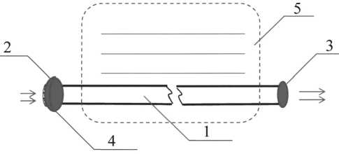
Fig. 4. Fiber optic substance sensor
The use of a fiber-optic substance sensor allows you to expand the scope of application, while simplifying the design and increasing the sensitivity of the sensor. A fiberoptic substance sensor containing a piece of fiber-optic cable, characterized in that it is equipped with a microlens and an object microlens, which are located at opposite ends of the fiber segment. -optical cable, and a film with the addition of carbon nanotubes deposited on the surface of the object microlens.
A method for obtaining a functional three-dimensional component of an optoelectronic device and a functional three-dimensional component of an optoelectronic device (RU 2731498 C1)
The group of inventions relates to a technology for producing semiconductor devices, and more precisely to a method for producing unsubstituted arrays of filamentary nanocrystals, as well as to the structure of a functional three-dimensional component made according to the claimed method and intended for use in optoelectronic devices. The invention can find application, for example, in the industrial production of light-emitting devices and photosensitive elements [9].
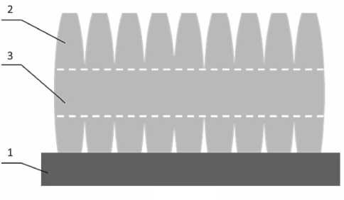
Fig. 5. A method for obtaining a functional three-dimensional component of an optoelectronic device
The method of obtaining a functional three-dimensional component (FTC) of an optoelectronic device (Fig. 5) is characterized by the fact that an array of unidirectional whisker nanocrystals (NW’s) of III-nitride materials is formed on the surface of a silicon substrate 1 heated to a temperature of 620–710оC by the method of molecular beam epitaxy. the formation of an array of nanocrystals 2 having a cross-section variable in height with thinning at both ends and partially intergrown in the mid-height zone 3, after which the obtained array is separated from the substrate by etching with an aqueous solution including hydrofluoric and nitric acid. The substrate-free NW’s array obtained by separation from the substrate is intended for use as a functional threedimensional component of an optoelectronic device. The functional three-dimensional component can be an array of nanocrystals of indium-gallium nitride, or indium nitride, or gallium nitride.
The technical result is to ensure the structural strength (integrity) of the FTC, formed in the form of an array of
REVIEW OF NANOTECHNOLOGICAL INVENTIONS
NW’s of III-nitride materials, sufficient for its functioning after separation from the substrate with a high optical quality of the NW material.
System for capturing gas containing volatile organic compounds and preparing carbon nanomaterials and method thereof (CN:201911384044:A)
The invention relates to a system for captor gas containing volatile organic compounds and preparing carbon nanomaterials and a method thereof, the system comprises an absorption/desorption subsystem, an adsorption/desorption subsystem and a carbonization subsystem, and comprises or does not comprise a gasliquid separation subsystem; the method for capturing the gas containing the volatile organic compounds and preparing the carbon nanomaterial by using the system comprises the following steps: firstly, removing most of the volatile organic compounds from the gas containing the volatile organic compounds through the absorption/ desorption subsystem; then, through the adsorption/de-sorption subsystem, realizing up-to-standard emission; when absorption or adsorption is close to saturation, executing desorption or desorption operation; condensing organic matters obtained by desorption or desorption in the gas-liquid separation subsystem, and collecting liquid (recycling or retreating);enabling the separated gas to enter a carbonization subsystem, generating a carbon nanomaterial at high temperature, after the tail gas of the carbonization subsystem and the tail gas of the ad-sorption/desorption subsystem are combined, and then discharging after reaching the standard. The use period of an adsorbent is prolonged, and the energy consumption is reduced; the volatile organic compounds are changed into carbon nanomaterials, so that the cost of the adsorbent is reduced [10].
Nano-coating protection method for electrical connectors (US20200291524)
Introduced here is a plasma polymerization apparatus and process [11]. Example embodiments include a vacuum chamber in a substantially symmetrical shape to a central axis. A rotation rack may be operable to rotate about the central axis of the vacuum chamber. Additionally, reactive species discharge mechanisms positioned around a perimeter of the vacuum chamber in a substantially symmetrical manner from the outer perimeter of the vacuum chamber may be configured to disperse reactive species into the vacuum chamber. The reactive species may form a polymeric multi-layer coating on surfaces of the one or more devices. Each layer may have a different composition of atoms to enhance the water resistance, corrosion resistance, and fiction resistance of the polymeric multi-layer coating.
Preparation method of nanometric size metal oxide additives that reduce the temperature of sintering and/or increase productivity in the manufacture of ceramic parts, improving mechanical properties without affecting the vitrification properties of ceramic bodies, tiles or coatings (US20200115287)
The object of this invention is a process for manufacturing, conditioning and stabilization of a family of base additives sodium, potassium, boron, silicon, zinc, calcium oxides, among others, prepared by physicochemical and chemical synthesis methods that form nanometric structures, reformulated with deflocculant, sequestrants and dispersants additives that allow to obtain a dispersion or powder capable to decrease the sintering temperature of a ceramic body due to the high fluxing power, which is maximized by the use of nanotechnology in the structures obtained [12].
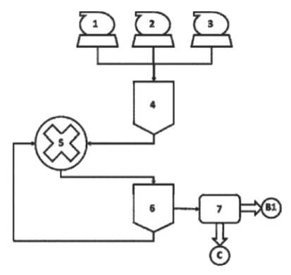
Fig. 6. Schematization of the process of preparation of nanostructures by means of a physicochemical process:
1. Raw material dosing system
2. Additive dosing system
3. Aqueous medium dosing system
4. Slurry preparation tank
5. High-energy mill
6. Dispersion tank
7. Storage of nanostructured additive in an aqueous medium
B1. Nanostructured additive in an aqueous medium goes to synthesis process by means of chemical route
C. Nanostructured additive in an aqueous medium goes to drying process
The process consists in the preparation of nucleation seeds of metal, silicates and carbonates oxides by means of a physicochemical process, and which allow nanometric structures to grow by means of a chemical pro-
REVIEW OF NANOTECHNOLOGICAL INVENTIONS cess in a chemical synthesis process wet basis of sodium, boron, silicon, zinc, potassium and calcium oxides. The combination of these oxides allows structuring elements of high fluxing power due to their high surface area and physicochemical composition. The additives prepared in this invention are chemically stabilized with deflocculating agents, which allow the additives to be incorporated into the aqueous medium grinding process of the ceramic body.
Applications made with the additives of this invention allow the sintering temperature of a red body to be reduced from 1150оC to 1000оC and in porcelain bodies from 1180оC to 1050оC, with the use of 0.2 to 5% of the additive, or increasing the speed of the heat treatment by up to 20%, and it can be used in the manufacture of bathroom fittings, molding parts, components for tooling, coatings, valances, enamels, vitrified pastes and other ceramic components. The present invention proposes several nanostructured additive formulations with high performance fluxing properties, which allow to optimize and standardize the sintering process and to improve the mechanical properties of the ceramic body. It also proposes different methods of application of the additive in ceramic formulations.
Tellurium nanorods, energy storage devices and preparation methods thereof, and method for preparing tellurium nanomaterials (CN:201910699049:A)
The invention discloses a tellurium nanorod, energy storage devices and a preparation method thereof, and a method for preparing tellurium nanomaterials, and relates to the field of preparation of thetellurium nanomaterials [13]. According to the method for preparing the tellurium nano materials, the preparation of the tellurium nano materials can be realized through a simple electrochemical strippingmethod only under normal temperature and normal pressure conditions, the preparation method is simple to operate, and the electrolysis equipment used is simple. The tellurium nanorods prepared by thepreparation method are onedimensional tellurium nanorods, can be widely applied to various energy storage devices, and have the advantage of high capacitance.
The specialists can also be interested in the following inventions related to nanotechnologies:
-
• Raw mixture for production of fine-grained polymer concrete modified by microsilica [14].
-
• Plant for synthesis of carbon-containing nanomaterials [15].
-
• Shear testing of composite materials at high temperatures [16].
-
• Method for producing silver nanoparticles [17].
-
• Emulsion system with nanoparticles for limiting water inflows into oil and gas wells [18].
-
• Method for producing nanocrystalline cubic tungsten carbide [19].
-
• Construction structural element [20].
-
• Study of deformation properties and fluidity of plastic lubricants with additives of various types of carbon nanostructures [21].
-
• Composition with carbon nanotubes to produce a carbon billet for high-density SiC/C/Si ceramics [22].
-
• Compositions containing nanometric copper [23].
-
• The preparation of ceramic composites by modification of carbon nanostructures [24].
-
• Composite membrane for drying natural and technological gas mixtures based on graphene oxide intercalated with hydroxylated fullerene derivatives [25].
-
• A method to produce modified carbon nanotubes [26].
-
• Functional element of a semiconductor device [27].
-
• Investigation of the effect of carbon nanotube functionalization on the conducting properties of a composite material [28].
-
• Charge based on aluminum oxide and a method for producing strong ceramics [29].
-
• Emulsion-suspension systems with nanoparticles for oil and gas wells maintenance [30].
-
• Solid-state supercapacitor with a dielectric layer made of dielectric nanopowder [31].
-
• Carbon ceramic fiber-reinforced composite material and method for its production [32].
-
• Investigation of impact rupture of polymer-tissue composites reinforced with carbon nanotubes [33].
-
• Method for producing nanoparticles of aluminum oxide [34].
CONCLUSION
One of the most challenging tasks the economy of every country face is to increase industrial competitiveness through technological upgrade. From the side of the state and companies the principal object to control in this process are the people and enterprises dealing with introduction of inventions and new technologies.
Therefore, we hope that the information published in this section will be in demand and useful for specialists.
REVIEW OF NANOTECHNOLOGICAL INVENTIONS
References Nanotechnologies: a review of inventions and utility models. Part IV
- Menshutina N.V., Lebedev A.E., Beloglazov A.P., Nesterov D.G. Thermal insulation material based on aerogel. Russian Federation Patent 2731479. 03.09.2020.
- Hristov D.A. A method of manufacturing core products with a basis of foamed polymers. Russian Federation Patent 2731930. 09.09.2020.
- Starkov V.V., Sedlovets D.M., Redkin A.N., et al. Method for the synthesis of graphene-like layers in porous silicon structures. Russian Federation Patent 2731278. 01.09.2020.
- Portnov E.L. Symmetrical four-pair cable with film-tube insulation of cores. Russian Federation Patent 2731624. 07.09.2020.
- Volkov Y.C., Salomatina E.V., Smirnova L.A. Method for alloying titanium dioxide with anatase allotropic modification of noble metal nanoparticles. Russian Federation Patent 2731277. 01.09.2020.
- Ivanov V.V., Efimov A.A., Khabarov K.M., et al. A method for manufacturing bulk micro-sized structures from nanoparticles. Russian Federation Patent 2730008. 14.08.2020.
- Tarasov B.P., Fursikov P.V., Fokin V.N., et al. Method for improving the efficiency of metal hydride heat exchangers. Russian Federation Patent 2729567. 07.08.2020.
- Afanasyev V.P., Bocharov G.S., Yeletsky A.V., et al. Fiber-optic substance sensor. Russian Federation Patent 2731036. 28.08.2020.
- Kotlyar K.P., Reznik R.R., Strom I.V., et al. Method for obtaining a functional three-dimensional component of an optoelectronic device and a functional three-dimensional component of an optoelectronic device. Russian Federation Patent 2731498. 03.09.2020.
- Available from: http://pss-system.cnipa.gov.cn/sipopublicsearch/insearch/showViewList.shtml
- Patentscope. US Patent 20200291524. Nano-coating protection method for electrical connectors. Available from: https://patentscope.wipo.int/search/en/detail.jsf?docId=US306235211&tab=NATIONALBIBLIO&_cid=P21-KFMO8A-99256-1.
- Patentscope. US Patent 20200115287. Preparation method of nanometric size metal oxide additives that reduce the temperature of sinterized and/or increase productivity in the manufacture of ceramic parts, improving mechanical properties without affecting the gresification properties of ceramic bodies, tiles or coatings. Available from: https://patentscope.wipo.int/search/en/detail.jsf?docId=US293242458&_cid=P21-KFMONA-04945-2
- Available from: http://pss-system.cnipa.gov.cn/sipopublicsearch/insearch/showViewList.shtml.
- Ivanov L.A., Demenev A.V., PisarenkoZh.V., Wang Q. Nanotechnologies: a review of inventions and utility models. Part III. Nanotechnologies in Construction. 2020; 12(3): 140–146. Available from: doi:10.15828/2075-8545-2020-12-3-140-146.
- Vavilov E.U. Installation for the synthesis of carbon-containing nanomaterials. Russian Federation Patent 2732842. 23.09.2020.
- Shangin K.V. Features of testing composition materials on shear at high temperatures. Information Technology Bulletin. 2020;1(23): 180–186.
- Nikiforova T.E., Smirnova A.A., Afonina I.A. A method for producing silver nanoparticles. Russian Federation Patent 2730824. 26.08.2020
- Sergeev V., Tanimoto K., Abe M. The Water-Blocking Agent with Improved Properties for IOR Implementation. European Association of Geoscientists & Engineers. Available from: doi:10.3997/2214-4609.201900162.
- Sivkov A.A., Shanenkov I.I., Shanenkova Yu.L. et al. A method of obtaining nanocrystalline cubic tungsten carbide. Russian Federation Patent 2730461. 24.08.2020.
- Ivanov L.A., Prokopiev P.S. The inventions in nanotechnologies as practical solutions. Part III. Nanotechnologies in Construction. 2019;11(3): 292–303. Available from: doi:10.15828/2075-8545-2019-11-3-292-303.
- Shilov M.A., Smirnova A.I., Gvozdev A.A. Rheology of Plastic Lubricants Containing Carbon Nanostructures. Journal of Friction and Wear. 2019; 40(6): 720-730.
- Shikunov S.L., Shikunova I.A., Kurlov V.N., Petkov I.S. Composition with carbon nanotubes for obtaining a carbon blank for high-density sic / c / si ceramics and a method for producing products from sic / c / si ceramics. Russian Federation Patent 2730092.17.08.2020.
- DE LA VEGA, Fernando; Melamed S. Compositions containing nanometric copper. Russian Federation Patent 2730285. 21.08.2020
- Paramonova N.D., Vartanyan M.A. Modification of Carbon Nanostructures for Obtaining Ceramic Composites (Review). Advances in Chemistry and Chemical Technology. 2019;33(4): 115-117.
- Brotsman V.A., Chernova E.A., Petukhov D.I. et al. Composite membrane for drying natural and technological gas mixtures based on graphene oxide intercalated with hydroxylated fullerene derivatives. Russian Federation Patent 2730320. 21.08.2020.
- Ivanov L.A., Bokova E.S., Muminova S.R., Katuhin L.F. Nanotechnologies: a review of inventions and utility models. Part I. Nanotechnologies in Construction. 2020;12(1): 27–33. Available from: doi:10.15828/2075-8545-2020-12-1-27-33.
- Kukushkin S.A., Osipov A.V., Svyatets G.V. Functional element of a semiconductor device. Russian Federation Patent 2730402. 21.08.2020.
- Garipov R. R., Khantimerov M. M., Suleymanov N. M. Investigation of the Effect for Carbon Nanotube Functionalization on the Conducting Properties of a Composite Material. Advanced Materials and Technologies. 2020; 1(17): 64-67.
- Nepochaev Yu.K., Bogaev A.A., Pletnev P.M., Malikova E.V. A charge based on aluminum oxide and a method for producing durable ceramics. Russian Federation Patent 2730229. 19.08.2020.
- 30.Sergeev V., Tanimoto K., Abe M. Innovative Emulsion-Suspension Systems Based on Nanoparticles for Drilling and Well Workover Operation. Society of Petroleum Engineers. Available from: doi:10.2118/197510-MS.
- Doroshkevich A.S., Shilo A.V., Zelenyak T.Yu. and others. Solid-state capacitor-supercapacitor with a dielectric layer made of dielectric nanopowder. Russian Federation Patent 2729880. 13.08.2020.
- Ivanov L.A., Prokopiev P.S. The inventions in nanotechnologies as practical solutions. Part IV. Nanotechnologies in Construction. 2019; 11(4): 447–457. Available from: doi:10.15828/2075-8545-2019-11-4-447-457.
- Kobzev V.A., Chechenin N.G., Bakunov K.A. Investigation of Impact Rupture of Polymer-Tissue Composites Reinforced With Carbon Nanotubes. Scientific Notes of The Faculty of Physics of Moscow University. 2020;2: 202-106.
- Kuzma-Kichta Yu.A., Ivanov N.S., Kiselev D.S., Lavrikov A.V. A method for producing nanoparticles of aluminum oxide. Russian Federation Patent 2730921. 26.08.2020.
