Novel Optimized Designs for QCA Serial Adders

Author: A. Mostafaee, A. Rezaei
Journal: International Journal of Information Technology and Computer Science(IJITCS) @ijitcs
Article in issue: 2 Vol. 9, 2017.
Free access
Quantum-dot Cellular Automata (QCA) is a new and efficient technology to implement logic Gates and digital circuits at the nanoscale range. In comparison with the conventional CMOS technology, QCA has many attractive features such as: low-power, extremely dense and high speed structures. Adders are the most important part of an arithmetic logic unit (ALU). In this paper, four optimized designs of QCA serial adders are presented. One of the proposed designs is optimized in terms of the number of cells, area and delay without any wire crossing methods. Also, two new designs of QCA serial adders and a QCA layout equivalent to the internal circuit of TM4006 IC are presented. QCADesigner software is used to simulate the proposed designs. Finally, the proposed QCA designs are compared with the previous QCA, CNTFET-based and CMOS technologies.
Quantum-dot cellular automata, QCA cell, Serial adder, QCADesigner, D flip-flop
Short address: https://sciup.org/15012618
IDR: 15012618
Text of the scientific article Novel Optimized Designs for QCA Serial Adders
Published Online February 2017 in MECS DOI: 10.5815/ijitcs.2017.02.05
According to the Moore’s law, every eighteen months, the number of transistors built on a chip doubles, which has been persisted as a law in electronic industry for more than fifty years [1-3]. Recently, current CMOS technology reaches to its physical limitations and faces challenging problems such as high power consumption and difficulties in feature size reduction. Thus, many researches have been conducted to find various technologies in order to replace the conventional CMOS technology. QCA is a new nanotechnology to implement logic circuits. Low power consumption and high processing speed are the advantages of this technology and it is possible to replace VLSI technology with QCA technology [4, 5]. In QCA, the QCA cells are used to implement logic circuits [6]. Adders are the most important part of an arithmetic logic unit (ALU). Several studies have been reported about adders [7-11] and QCA serial adders [12-14]. Three designs of QCA serial adders have been presented in the previous studies [12-14]. These designs have been implemented using coplanar crossing method and have not been optimized in terms of cell count, occupied area and input to output delay. In this paper, three new designs and one optimized design of QCA Serial adder are presented. The first design, which is implemented using a full adder and a D flip-flop without any wire crossing methods, is optimized in terms of cell count, area and delay. Also, two new designs of QCA serial adder are introduced, which are implemented using full adder, D flip-flop, shift register and JK flipflop. The last design is the QCA implementation of the internal circuit of TM4006 IC. The rest of this paper is organized as follows: Section II introduces the QCA technology. In Section III, the proposed QCA serial adders are presented. The simulation results and comparisons are shown in Section IV. Finally, Section V concludes the paper.
-
II. I ntroduction to QCA
QCA technology first introduced by Lent in 1994 [4]. In this section, the basis of QCA, its main logic Gates and clocking of QCA circuits are described.
-
A. QCA Cell
QCA is based on the QCA cell. The QCA cell is composed of one square with 4 quantum dots and two free electrons as shown in Fig.1 [15-17]. As a result of columbic interaction between the free electrons, they will tend to occupy diagonally opposite into the dots in only two possible states. These two possible states are denoted as the cell polarization P=+1 to represent logic “1” and P=-1 to represent logic “0” as shown in Fig.1. All logic circuits can be implemented in QCA technology using the inverter Gate, majority Gate and wires [18].
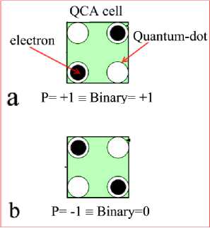
Fig.1. QCA cell (a) Logic “1” (b) Logic “0”.
-
B. QCA wire
Wire is used in order to transfer data. Due to electrostatic interaction between the adjacent QCA cells, binary data can be transferred from input to output. There are two types of wires in QCA: binary wire (90 degree wire) and inverter chain (45 degree wire) as shown in Fig.2.
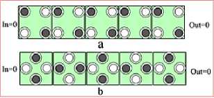
Fig.2. QCA (a) binary wire, (b) inverter chain.
-
C. QCA wire-crossing
In QCA, there are two types of crossovers (wirecrossing) i.e. overlapping of wires: coplanar and multilayer crossovers as shown in Fig.3. Coplanar crossover uses single layer and two wire types (binary wire and inverter chain), but the multilayer crossover uses binary wire and more than one layer of cells.
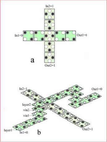
Fig.3. (a) Coplanar crossing, (b) multilayer crossing.
-
D. Majority Gate
This Gate is composed of five QCA cells (three inputs and one output cells). The majority Gate produces the following function at its output:
F = M ( A, B , C) = A. B + A.C + B . C (1)
Where A, B and C are the inputs and F is the output of the majority Gate. According to the output equation, if at least two inputs have a specific logic level then the output follows them. In Fig.4 the QCA layout, circuit diagram and simulation results of the majority Gate using QCADesigner are shown.
-
E. AND and OR Gates
Using the majority Gate, AND and OR Gates can be realized. If one input of a 3-input majority Gate is set to logic “0”, the majority Gate behaves like an AND Gate. If one input is set to logic “1” ”, the majority Gate behaves like an OR Gate. In Fig.5 and Fig.6, the QCA layout, circuit diagram and simulation results of these AND and OR Gates are shown.
-
F. Inverter Gate
The inverter or NOT Gate is shown in Fig.7, where its input is inverted due to the different polarizations, which are misaligned between the corners of the cells. Inverter Gate has different designs. In Fig.7, the QCA layout, circuit diagram and simulation results of some possible implementations of QCA inverter Gate are shown.
-
G. QCA clocking
The clock signal in QCA technology is different from the clock signal in CMOS technology. In QCA, clock signal is used to control and synchronize QCA circuits and also to provide the necessary power to run the circuit. There are four clock signals in QCA technology and each clock signal is composed of four phases (Switch, Hold, Relax and Release) [19, 20]. In QCADesigner software, clock signals are shown in the different colors [21] (Green color for Clock 0, violet color for Clock 1, blue color for Clock 2 and white color for Clock 3). Fig.8 shows the QCA clock signals.
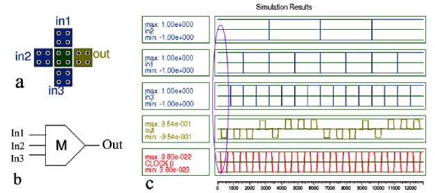
Fig.4. Majority Gate (a) QCA layout (b) circuit diagram (c) simulation results.
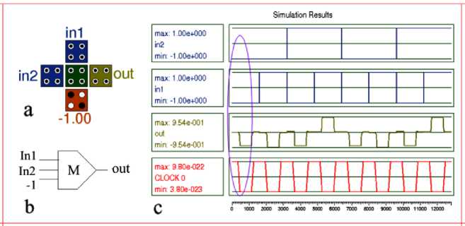
Fig.5. AND Gate (a) QCA layout (b) circuit diagram (c) simulation results .
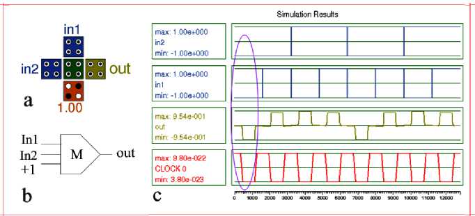
Fig.6. OR Gate (a) QCA layout (b) circuit diagram (c) simulation results.
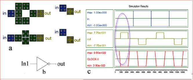
Fig.7. Inverter Gate (a) QCA layouts (b) circuit diagram (c) simulation results.
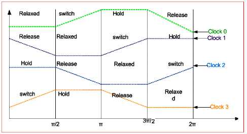
Fig.8. QCA clocking.
-
III. P roposed QCA S erial A dders
In this section we present three new designs and one optimized design of QCA serial adders. QCADesigner software is used to design and simulate the proposed layouts.
-
A. The first proposed design
This serial adder is composed of one full adder and one D flip-flop. A D flip-flop can be implemented by a QCA wire with four clock signals [22]. In order to design a D flip-flop circuit in VLSI technology, distinct clock signal (CLK) must be used. In QCA, each cell can has a different clock signal so in QCA unlike VLSI technology there is no need to have a separate input as CLK. Fig.9 shows the circuit diagram and QCA layout of a D flipflop. Also, in order to implement QCA full adder, three majority Gates and two inverters are applied [23]. In Fig.10 the circuit diagram and QCA layout of a full adder are shown. In the first serial adder, carrier output signal is connected to the input of D flip-flop, and then the output of D flip-flop is used as one of the inputs of full adder. The QCA layout of this serial adder and its circuit diagram are shown in Fig.11. This design are implemented with 48 cells and the delay from the input to the output is four clock phases and its approximated area is 0.03 µm2. In addition, this circuit has been implemented without any wire-crossing methods.
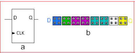
Fig.9. QCA D flip-flop (a) circuit diagram (b) layout.
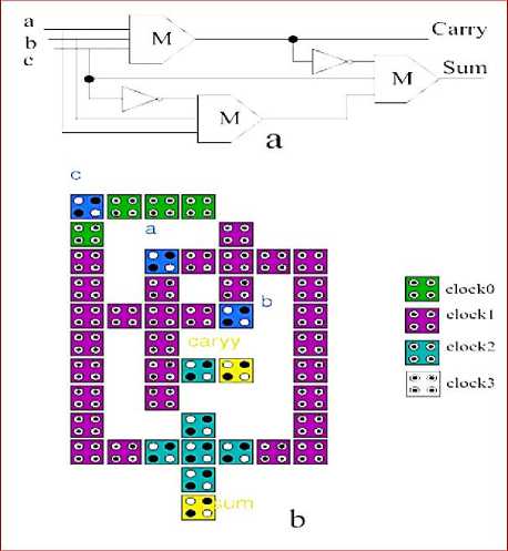
Fig.10. QCA full adder (a) circuit diagram (b) Layout.
-
B. The second proposed design
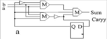
This is a new design of QCA serial adder, which is composed of two shift registers, one full adder and one D flip-flop. A shift register can be implemented by a D flip flop [22]. Fig.12 shows the circuit diagram of a 4-bit shift register, its QCA layout and its simulation results using QCADesigner software. The circuit diagram and QCA layout of the second proposed QCA serial adder are shown in Fig.13 [24]. In this circuit, the outputs of shift register 1, shift register 2 and D flip-flop are connected to Z, Q and X inputs, respectively (the inputs of full adder). The output signal “sum” is connected to the shift register 1 as a serial input, and the output signal “carry” is connected to the input of D flip-flop. The clocking in CMOS technology is different from QCA, so to implement this circuit in QCA, the clock signal and displacement control can be removed from the circuit. This serial adder is implemented using 218 QCA cells. The delay is twenty clock phases from the input to the output and its approximated area is 0.206 µm2. Also, it is implemented in two layers.
ГтетНИ[^1СТС1|^1
Кет Кет КетКет Кет
Я а № пет m ty ~> 41 гж-141
нет кет пг1 m m m пттп qq мет__Вы
[йтп^щщщр^ щ етет [-д-1
мет №1
ь
Fig.11. The first proposed QCA serial adder (a) circuit diagram (b) layout.
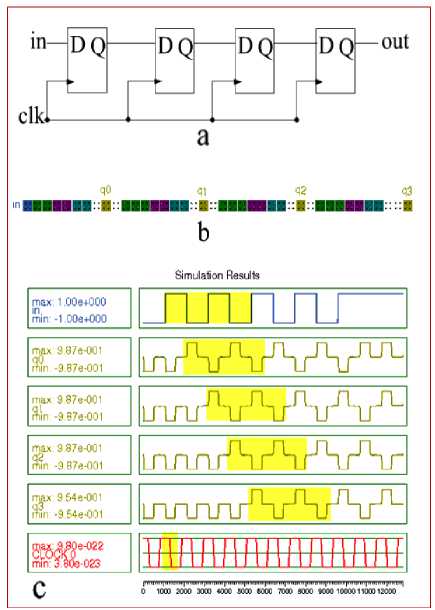
Fig.12. 4-bit shift register (a) circuit diagram (b) QCA layout (c) simulation results.
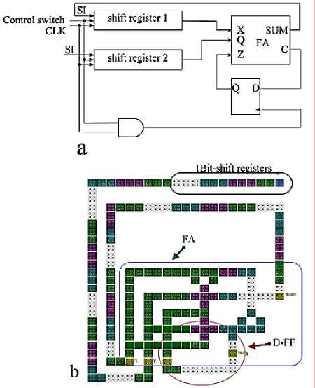
Fig.13. The second proposed QCA serial adder (a) circuit diagram (b) layout.
-
C. The third proposed design
This circuit is almost similar to the previous designs. In this design, XOR Gate and JK flip-flop are used instead of the full adder and D flip-flop in the previous design, respectively [24]. The circuit diagrams and QCA layouts of XOR Gate and JK flip-flop are shown in Fig.14 and Fig.15, respectively [22, 25]. Fig.16 shows the circuit diagram and QCA layout of the third proposed QCA serial adder. This QCA layout is implemented using 420 cells in two layers. Its approximated area is 0.487 µm2, also the input to output delay is 28 clock phases.
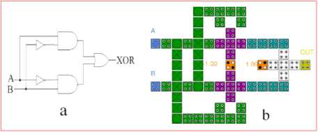
Fig.14. XOR Gate (a) block diagram (b) QCA layout.
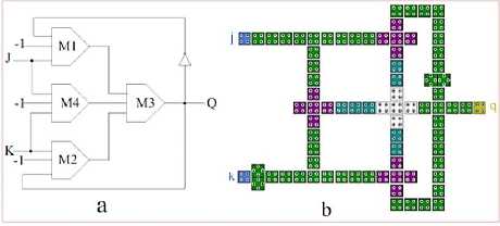
Fig.15. JK flip-flop (a) block diagram (b) QCA layout.
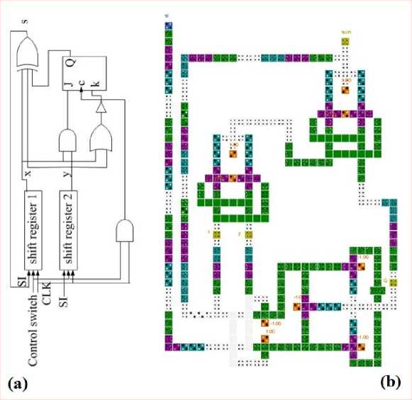
Fig.16. The third proposed QCA serial adder (a) circuit diagram (b) layout.
-
D. The fourth proposed design
This design is based on the internal circuit of Tm4006
IC. Tm4006 is a serial adder integration circuit. The internal structure of TM4006 IC is shown in Fig.17a. This circuit composed of XOR, OR, AND and NOT Gates and D flip-flop. The inputs are Cb-1, A, B, Cb and the output is sum. The carry signal Cb is connected to the input of D flip-flop and the output of D flip-flop is connected to the input Cb-1. If nsub is logical “1”, the circuit works as an adder, and if nsub is logical “0”, the circuit works as a subtractor. The QCA layout of this serial adder is shown in Fig.17b. This layout is implemented using 638 QCA cells in three layers and its approximated area is 0.75 µm2. Also, its input to output delay is 12 clock phases.
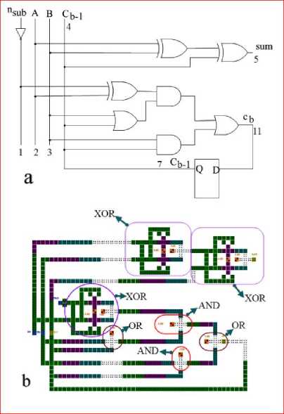
Fig.17. The fourth proposed QCA serial adder (a) circuit diagram (b) layout.
-
IV. R esults and D iscussion
To evaluate the functionality of the proposed designs, we have simulated them by QCADesigner software 2.03 [21]. This tool makes the design, layout and simulation of QCA circuits easier and faster by supplying powerful CAD characteristics. The default parameters of the both engines of QCADesigner (bi-stable and coherence-vector simulation engines) were used and same results were achieved, which indicate the correctness of the proposed designs. The input and output waveforms for the proposed designs shown in Fig.11, Fig.13, Fig.16 and Fig.17 are shown in Fig.18, Fig.19, Fig.20 and Fig.21, respectively. These figures are obtained using the following parameters in the Bistable approximation engine [21]: Number of samples 128000, Convergence tolerance 0.001, Radius of effect 65nm, Relative permittivity 12.9, Clock high 9.8e-22J, Clock low 3.8e-23J, Clock amplitude factor 2, Layer separation 11.5nm, Maximum iterations per sample 100 and randomize simulation order. Also, cells are assumed to have a width and height of 18 nm and quantum dots have 5 nm
diameter. The comparison between the proposed QCA serial adders and the previous works in terms of wire-
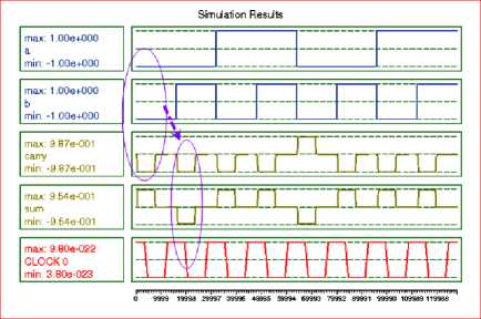
Fig.18. Simulation results of the first proposed QCA serial Adder.
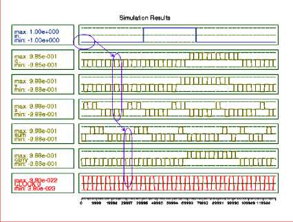
Fig.19. Simulation results of the second proposed QCA serial Adder.
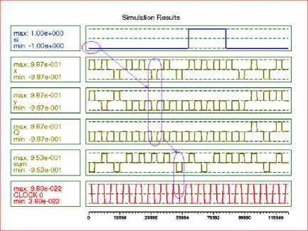
Fig.20. Simulation results of the third proposed QCA serial Adder crossing types, cell count, area and delay is shown in Table 1. As shown in Table 1, the previous layouts in [12-14] have been designed using the coplanar crossover scheme. In comparison with [12], the important improvements for the first proposed design shown in Fig.11 are 69% and 52% in the area and cell count, respectively. Where, the important improvement (II) is obtained by the following equation [26]:
II = (1 - x ) x 100 y
Where x and y stand for the measured objects (area or cell count) for our designs and the previous works, respectively.
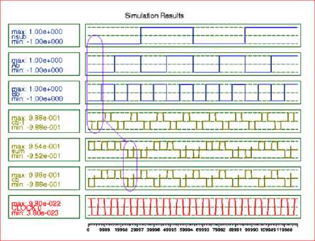
Fig.21. Simulation results of the fourth proposed QCA serial Adder.
Also, in comparison with the previous work presented in [13], the important improvements are 95% in area and 88% in cells count. In comparison with [14], the important improvements are 84% in the area and 69% in cells count. In addition, our best design is implemented without any wire-crossing methods, which is an important advantage over the previous works. Moreover, in the best proposed design, the input to output delay is four clock phases, which is faster than the previous designs. Also, we have compared our best QCA design with the previous CMOS implementations. Fig.22 shows an equivalent CMOS layout of the proposed serial adder shown in Fig.11. This layout is implemented with 45nm
CMOS technology and its approximated area is 12.8 µm2, which is 427 times bigger than the QCA layout shown in Fig.11. Table 2 shows the comparison between our QCA designs with the previous CNTFET-based designs. As it can be seen from Table 2, the QCA design has 14 x 10 8 times less than than the 32nm CNTFET-based ternary serial adder presented in [27] in power consumption and also, its occupied area is 114 times smaller. Also, in comparison with the CNTFET-based ternary Full adder presented in [28], our best QCA design is more than 166 times faster. Also, it has power consumption approximately 11 x 10 8 times less than [29]. From these results, it is clear that the QCA designs are more efficient in terms of area, power and delay in comparison with the other technologies. The obtained results show that the proposed QCA serial adders work satisfactorily and produce the required results. The implementation of these designs may lead to the efficient use of complex circuits in the various applications, which may be a future technical advancement of this work.
Table 1. Comparison with the previous works.
References Novel Optimized Designs for QCA Serial Adders
- G.E., Moore, “Cramming more components onto integrated circuits”, Electronics, vol. 38, no. 8, pp. 114, 1965.
- R. Robert, “Moore's law: past, present and future”, Spectrum, IEEE, vol. 34, no. 6, pp. 52-59, 1997.
- International Technology Roadmap for Semiconductors, Jointly Sponsored by European Semi-conductor Industry ASSC, Japan Electronics and Information Technology Industry ASSC, 2016.
- C.S. Lent, P.D. Taugaw, W. Porod, “Quantum Cellular Automata,” Iopscience, vol. 4, no. 1, pp. 175-245, 1993.
- R. Compano, L. Molenkamp, D.J. Paul, “Technology Roadmap for Nanoelectronics,” Proceeding of the European Commission IST Programme, Future and Emerging Technologies, Conference, 1999.
- C.S. Lent, P.D. Taugaw, W. Porod, “Bistable saturation in coupled quantum dots for quantum cellular automata,” Applied Physics Letters, vol. 62, no. 7, pp. 714-716, 1993.
- V.G. Deibuk, A.V. Biloshytskyi, “Design of a Ternary Reversible/Quantum Adder using Genetic Algorithm”, International Journal of Information Technology and Computer Science (IJITCS), vol. 9, pp. 38-45, 2015.
- A. Sajid, A. Nafees, S. Rahman, “Design and Implementation of Low Power 8-bit Carry-look Ahead Adder Using Static CMOS Logic and Adiabatic Logic”, International Journal of Information Technology and Computer Science (IJITCS), vol. 11, pp. 78-92, 2013.
- M. Hayati, A. Rezaei, “Design of novel efficient adder and subtractor for quantum-dot cellular automata”, International Journal of Circuit Theory and Applications, vol. 43, no 10, pp.1446-1454, 2015.
- H. Bandani Sousan, M. Mosleh, S. Setayeshi, “Designing and Implementing a Fast and Robust Full-Adder in Quantum-Dot Cellular Automata (QCA) Technology”, Journal of Advances in Computer Research, vol. 6, no. 1, pp. 27-45, 2015.
- R.R. Devi, S. Thilakavathi, K.M. Suganya, “Clock Zone Based QCA Adder Architecture Design”, International Journal of Advanced Research in Computer Science and Software Engineering, vol. 5 , no. 10, pp. 560-563, 2015.
- I. Hänninen, J. Takala. “Binary Adders on Quantum-Dot Cellular Automata,” Journal of Signal Processing Systems, vol. 58, no. 1, pp. 87-103, 2010.
- T. Suratkar, “QCA Based Design of Serial Adder,” ITSI-TEEE, vol. 1, no. 5, pp. 57-61, 2013.
- K. Walus, G.A. Jullien, V.S. Dimitrov, “Computer arithmetic structures for quantum cellular automata,” Proceedings of the IEEE Conference on Nanotechnology, vol. 2, pp. 1435-1439, 2004.
- S. Shin, G. Lee and K. Yoo, “Design of Exclusive-OR Logic Gate on Quantum-Dot Cellular Automata,” International Journal of Control and Automation, vol. 8, no. 2, pp. 95-104, 2015.
- K. Walus, G. Schulaf, G.A. Julliaen, “High Level Exploration of Quantum Dot Automata,” Proceedings of the IEEE Conference on Nanotechnology, vol. 1, pp. 30-33, 2004.
- K. Walus, W. Wang, G.A. Julliaen, “Quantum Cellular Automata Adders,” Proceedings of the IEEE Conference on Nanotechnology, vol. 2, pp. 461-464, 2003.
- I. Amlani, O. Orlov, G. Toth, G.H. Bernstein, C.S. Lent, G.L Snider, “Digital Logic Gate Using Quantum-Dot Cellular Automata,” Science, vol. 284, no. 5412, pp. 289-291, 1999.
- H. Cho, E.E. Swartzlander, “Adder designs and analyses for quantum dot cellular automata,” IEEE Trans, Nanotechnol, vol. 6 no. 3, pp. 374-383, 2007.
- S. Hashemi, M. Tehrani, K. Navi, “An efficient quantum-dot cellular automata full-adder,” Academic journals, vol. 7, no. 2, pp. 177-189, 2012.
- QCADesigner, Available: http://mina.ubc.ca/qcadesigner, 2016.
- L. Lim, A.Ghazali, S.C.T. Yan, C.C. Fat, “Sequential circuit design using Quantum-dot Cellular Automata (QCA),” IEEE International Conference on Circuits and Systems (ICCAS), pp. 162-167, 2012.
- A. Mostafaee, A. Rezaei, M.M. Karkhanehchi, S.M. Jamshidi, “Design of QCA Full Adders without Wire Crossing,” Boson Journal of Modern Physics, vol. 2, no. 2, pp. 90-96, 2015.
- M. Mano, “Digital Design,” California State University, Los Angeles, 2011.
- M.R. Beigh, M. Mustafa, F. Ahmad, “Performance Evaluation of Efficient XOR Structures in Quantum-Dot Cellular Automata (QCA),” Scientific Research, vol. 4, no. 2, pp. 147-156, 2013.
- M. Hayati and A. Rezaei, “An efficient and optimized multiplexer design for quantum-dot cellular automata,” Journal of Computational and Theoretical Nanoscience, vol. 11, no. 1, pp. 297-302, 2014.
- M. H. Moaiyeri, M. Nasiri, N. Khastoo, “An efficient ternary serial adder based on carbon nanotube FETs,” Engineering Science and Technology, vol. 19, no. 1, pp. 271-278, 2016.
- S.A. Ebrahimi, P. Keshavarzian, S. Sorouri, M. Shahsavari, “Low power CNTFET-based ternary full adder cell for nanoelectronics,” Int. J. Soft Comput, Eng, vol. 2, no. 2, pp. 291–295, 2012.
- P. Keshavarzian, R. Sarikhani, “A novel CNTFET-based ternary full adder,” Circuits Syst Signal Processing, vol. 33, no. 3, pp. 665-679, 2014.
