Optical Packet Switch Architectures: A Comparative Study

Author: Preeti Singh, Seema Verma
Journal: International Journal of Information Technology and Computer Science(IJITCS) @ijitcs
Article in issue: 11 Vol. 4, 2012.
Free access
In this paper four fiber-loop-buffer based photonic packet switched architectures are compared. It is done in terms of their packet loss probability and their optical cost under various load conditions for the random traffic model. The recirculating type delay lines are used for the storage of packets to resolve the contention. The architectures use semiconductor optical amplifiers(SOAs) and tunable wavelength converters(TWCs) in the recirculating loop buffer. The architectures have advantage of simultaneous Read/Write and, wavelength reallocation using TWCs in the recirculating loop buffer. Therefore, it improves the switch performance over the architectures using SOAs in the loop buffer. The cost of the various architectures is evaluated by considering FCC (fiber-to-chip coupling) and the WSU (wavelength speed up factor) model.
Photonic Packet Switching, Packet Loss Probability, Optical Cost, Load
Short address: https://sciup.org/15011785
IDR: 15011785
Text of the scientific article Optical Packet Switch Architectures: A Comparative Study
Published Online October 2012 in MECS
This paper is organized as follows: Section 2 gives structure of optical packet switched networks Section 3 describes the related work. Section 4 presents the cost analysis of the optical packet switch architectures. Results and conclusions are given in the final section.
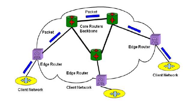
Fig. 1: Schematic of the generalized optical networks
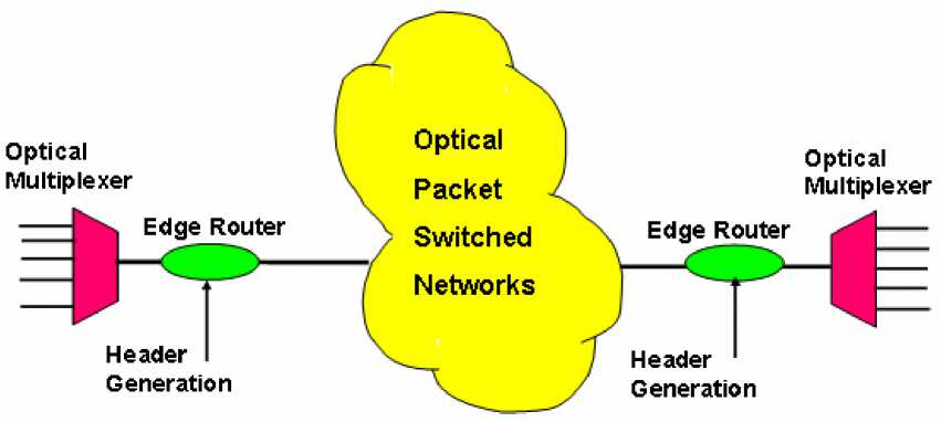
Fig. 2: Schematic of the aggregated core networks
-
II. Structure of Optical Packet Switched Networks
The generic layout of the network is shown in Figure 1. The edge routers acting as an interface between clients and core network lie on the periphery of the network cloud. Core as well as edge routers are electronic in nature. It is not possible to handle high data rate with these electronic routers hence, possessing speed limitations. To overcome this problem aggregate core transport networks as shown in Figure 2 came in to picture. The packet header is processed electronically at a slower rate, while the payload is processed optically at a higher rate [15] . The motivation to build the optical packet switch is when ingress node (edge router) aggregate the large number of packets optically for a very high bit rate payload, as the data is generated by the electronic sources. The switch in the core network will convert the low bit rate header of the packet (attached with a high bit rate payload) in electronic domain and maintains the payload in optical form. Routing of the packet is done as per the information stored in the header. The aggregated packet can be separated optically and passed in to the client network as soon as it reaches the egress node i.e. the edge router at which packet exists the core network.
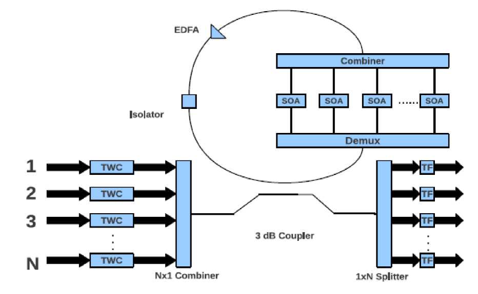
Fig. 3: Schematic of loop buffer architecture A1
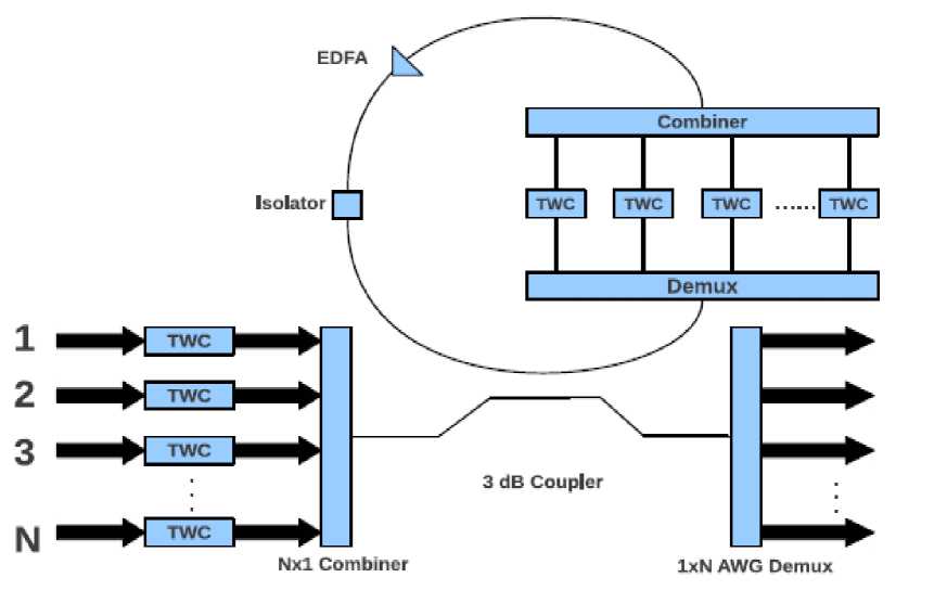
Fig. 4: Schematic of loop buffer architecture A2
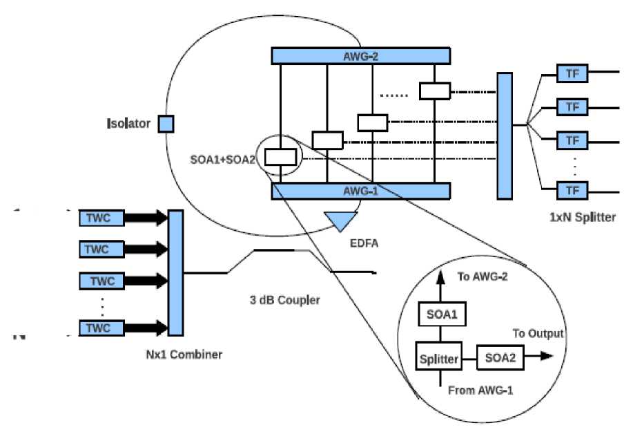
Fig. 5: Schematic of loop buffer architecture A3.
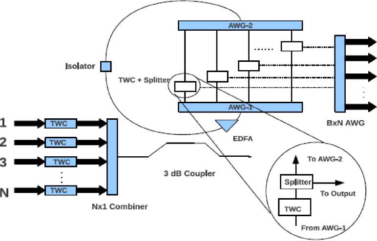
Fig. 6: Schematic of loop buffer architecture A4
-
III. Related Work
-
2. Wavelength reallocation: Buffering is used for contention resolution. Storage time can be adjusted by changing the number of circulations. However there is a limit on the maximum number of circulations [18] . One of the factors responsible for this limit is cross talk. To reduce the noise due to cross talk dynamic wavelength reallocation is used which result in an increase in maximum buffering time. This wavelength conversion also reduces packet loss probability [19] . To minimize cross talk in DWDM networks TWCs has been used as buffer gates. This is possible in architectures A2 and A4 only.
-
3. Control complexity: It does the processing of routing information, updates header information, forwards header to output interface, tracking buffer and input-output port status, synchronization of operation of switch components with master clock in reference, communication with other switching nodes etc. It is implemented electronically and the actual data transmission takes place optically. It depends on the photonic components requiring synchronized control. In architectures A2 and A4 only two components, input and buffer TWCs, have to be controlled so it’s control complexity is lowest. The control complexity of the architectures A2 and A4 is lowest as only two components, input and buffer TWCs, have to be controlled. For architecture A1,three components-the input TWCs, buffer SOAs, and output TFs have to be controlled, so it’s control unit complexity is moderate. . In architecture A3 four components, i.e., input TWCs, two buffer SOAs, and TFs at the output have to be
-
4. Number of components: The cost of architectures depends on the number and type of components. The physical loss in the architectures can also be calculated by considering the insertion loss of each device. Number of components are lowest in architecture A2 and highest for architecture A3.
-
5. Buffer utilization: Buffering is used for contention resolution. Optical buffer is one of the critical component of optical packet switching. Current optical buffers are mainly based on fiber delay lines which delay the packets rather than to store them.
-
6. For the architectures A1 and A2 the buffer capacity ( B ) can be fully utilized, but for the architectures A3 and A4, the buffer capacity is shared by the directly transmitted and buffered packets. Between the architectures A1 and A2, the
-
7. Packet loss probability: Packet loss is the failure of one or more transmitted packets to arrive at their destination.
The switch architectures (A1-A4) are shown in Figure 3-6 [16] . They consist of N TWCs, one at each input. The TWCs are tuned in every time slot to appropriate wavelength to place a packet in the loop buffer for avoiding contention. The Architecture A1 (Figure 3) proposed by Bendelli et al. [7] has SOA as gate switches in recirculating loop buffer for a specified number of wavelengths. The architecture A2 (Figure 4) proposed by Srivastava et al. [9] contain tunable wavelength convertors (TWCs) inside the buffer, which can resolve contention among the packets in wavelength domain. The architecture A3 was proposed by Choa et al. [12] . In A3 demux and combiner used in buffer loop of A1 and A2 are replaced by AWG demultiplexer (AWG-1) and AWG multiplexer(AWG-2). Two SOA gates are placed in each branch of the AWGs of the buffer. Figure 6 depicts the architecture proposed in [16]. All the architectures are designed for equal length packets. The packets are assumed to be frame aligned when they arrive at the input of the switch [17] . These architectures use recirculating-type delay lines for the storage of packets.
These four architectures can be compared in terms of their functionalities as :
controlled by the control unit, so the control unit complexity is very high.
latter utilizes the buffer capacity more effectively, as for this architecture simultaneous read-write operation is possible that is not possible for the architecture A1.
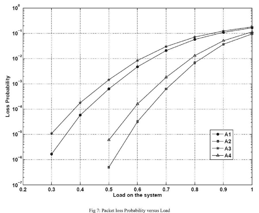
Considering the Random Traffic Model, packet loss probability for the switch configuration , under various load conditions has been examined using computer simulation. In Figure 7 packet loss probability versus load on the system is plotted for different buffer architectures for the random traffic model [16] .
Further the architectures can also be compared in terms of their Packet loss probability and cost. In the cost analysis of the architectures two models have been considered namely fiber-to-chip coupling (FCC) and wavelength speed-up model (WSU).
-
IV. Cost Analysis of the Optical Packet Switch Architectures
In this paper four optical packet switch architecture have been discussed. These architectures have their advantages over the other. One of the most important issue is the cost of these architectures. The, cost estimation of the architecture is not straight forward. The first compact model which is helpful in the estimation of the cost of the architectures was proposed by Caenegem [20]. The proposed cost model is based on fiber-to-chip coupling (FCC) which is the number of interconnections to the outer world through the component, where the cost of optical components is obtained by counting the number of FCC. The model assumes fix cost for the passive and active devices. Therefore, the cost of the optical components can be written as,
Ctwc ah
C opticaldevice = InPUt fiber's + Output fibers
Where, a is a normalization constant, h is the conversion range and b is wavelength speed-up characterization parameter which characterizes the cost of the TWC and its values lies between 0.5 to 5. The cost of the TWCs which can be tuned to wavelengths will be given by,
Thus, cost of the TWC which can be tuned to W wavelengths is assumed to be 4 (3 input fiber + 1 output fiber). The optical cost of the various devices in terms of FCC is presented in Table 1
С = { aW , TWC I
a ,
W > 1
W = 1
Table 1: Optical cost of the various devices using FCC method
|
Symbol |
Representation |
Cost |
|
c „ TWC |
Cost of the TWC |
4 |
|
^ N X1 Combiner |
Cost of the Combiner |
N +1 |
|
p N x 1 C Splitter |
Cost of the Splitter |
N +1 |
|
c 3 dB |
Cost of 3 dB Coupler |
4 |
|
p N x 1 Demux |
Cost of the Demux |
N +1 |
|
/^ N x 1 C Mux |
Cost of the Mux |
N +1 |
|
C . EDFA |
Cost of the EDFA |
2 |
|
c ISO |
Cost of the Isolator |
2 |
|
C Re ge |
Cost of the Regenerator |
21 |
|
c SOA |
Cost of the SOA |
2 |
|
c FBG |
Cost of the FBG |
2 |
|
^N xN CAWG |
Cost of the AWG |
2 N |
|
c FF |
Cost of the FF |
2 |
|
c TF |
Cost of the TF |
2 |
|
N C Cir |
Cost of the Circulator |
N |
|
C F |
Cost of the Fiber |
2 |
|
C Or |
Cost of the Optical reflector |
2 |
As per the cost model presented in [22] the maximum possible value of a is one. Therefore, TWCs which can tune to one wavelength only will cost unity. The cost model is further modified by considering the concept of LRWC (limited range wavelength converter) and FRWC (full range wavelength converter) and it is concluded that the value of the speed up factor should be in between 0.5 and 1. Further detailing can be found in [23].
4.1 Cost Estimation of the Architectures
In this section, optical cost of various architectures is computed. The total costs of the various architectures are computed by counting the cost of the all the devices needed to realize each switch structure. The cost of different architectures is computed by breaking the each architecture in three separate units as input, buffer and output where the cost of each unit will be given as Cin Cloop and Cout respectively. The cost of the architecture A1 can be computed as,
The cost of the input unit which consists of TWCs and combiner can be written as,
c = NC in + CN X 1 ^ in TWcTWC + CoCom
The cost of the output unit which consists of splitter and tunable filter will be given by,
c ,=c 1X,N w out Splitter TF
As this model assumes fixed cost, this model does not include the wavelength speed-up factor (WSU). To incorporate the effect of wavelength conversion, a heuristic cost model is proposed in [21] where the cost of the TWC’s is given by the expression
Similarly, the cost of the buffer unit will be given by,
C =C + C 1X B + + CB X1
Cloop C 3 dB + CDemux + BCSOA + CCom
+ Cm + C C + C EDFA ISO F
ctwc ah
Here, a is a normalization constant, h is the conversion range. Thus, the cost of the TWC which can be tuned to W wavelengths will be given by,
C twc = aW
In the notation, cost of each component is represented
Cq as p where p shows the component type and q is size/position of the device. In the subsequent cost equations buffer is represented as bu. Similarly, the costs of the architecture A2 can be modeled as,
The model assumes linear trend in cost with respect to the tunable wavelength range. In [22] , a relatively more generalized model have been presented where cost is given as,
С = МГin , + C N X1 in 1 N t^TWC + ^ Com
■r __ z-i 1x N out Demux
1X в bu B X1
Cloop C 3 dB + CDemux + BCTWC + CCom +
CEDFA + C BO + CF
The costs of the architecture A3 is given by the expression,
C = NC in + C N X1 in TWC + Com
|
C A 1 |
in TWC |
+ 4 N + 4 B + 14 |
(18) |
|
C A 2 |
in TWC |
+ BC buc + 2 N + 2 B + 2 B + 14 |
(19) |
|
C A 3 |
in TWC |
+ 4 N + 10 B + 15 |
(20) |
|
C A 4 |
in TWC |
+ BC buc + 4 N + 6 B + 11 |
(21) |
c c1X N + cNN + NC out Demux Splitter TF
C ooop = C 3 dB + C EDFA + C DU + B ( Ciittrr
+ 2С ) + С B X1 + С + С
+ SoSO) ) + Mux + ISO +
The costs of the architecture A4 can be expressed as,
c = NCin „ + C N X1
in TWC + Com
C out
1B B Х N + NC_ Demux TF
C ooop = C 3 dB + C EDFA + C D X Bmux + B ( C ^WC + C Sitter. ) + C Mx + C iso + C,
The optical costs of the different components using FCC methods are tabulated in Table 1. After applying the cost of the different components the cost of the various architectures will be given by the expressions,
In the next two sections cost of the architecture are evaluated numerically, by considering N=4 and B=8 using the two models.
4.2 Cost of the Architectures using FCC Method
In Figure 8, the costs of the architectures are evaluated by considering FCC model. The cost of the TWC is assumed to be 4 which is independent of the tunable range of the TWCs. Here the cost of the architecture A3 is highest (127 units). The cost of the architecture A3 and A4 is comparable to each other similarly the cost of A1 and A2 is comparable to each other. The FCC cost model does not take into account of tunable range of the TWCs, therefore higher cost of the architecture can be considered as direct measure of the number of components or size of the components to realize the switch architecture. It should be noted that more number of components with larger switch size will add to the cost.
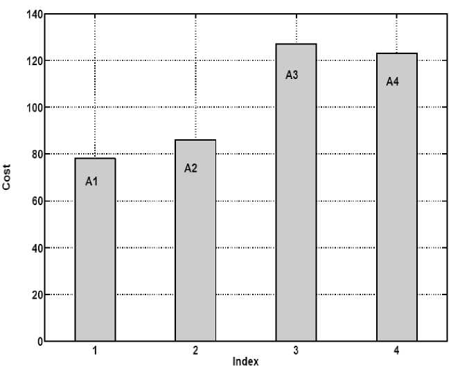
Fig. 8: Total cost of the various architectures using FCC method
4.3 Cost of the Architectures Using Wavelength Speedup Model (WSU)
In Figure 9, the cost of the various architectures are shown using WSU model. This model modifies the cost of the TWC by taking into accounts its tunable range. Here, three values of cost characterization parameter ( b
= 0.5, 0.7 and 0.9) are considered. For b = 0.5, the cost of the architecture A3 is highest (123 units). The following observations can be made from Figure 6,the cost of the architecture A2 and A4 are comparatively higher in comparison to architecture A1 and A3. It can also be observed that as the value of speed-up factor ( b )
increases, the cost of the architectures which have larger b(<0.7) the cost of the architecture A1 and A2 are number of TWC increases. For reasonable value of comparable to each other.
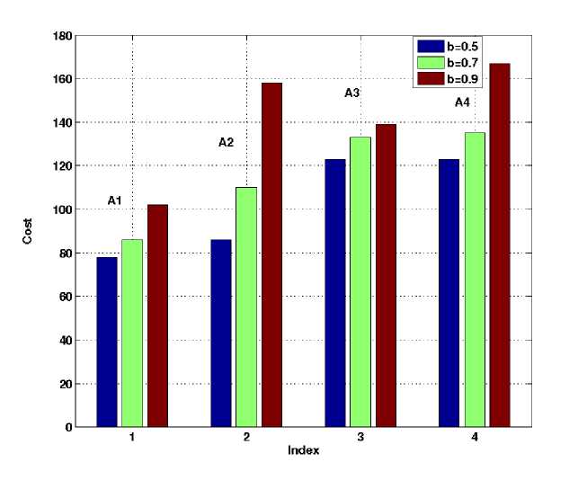
Fig. 9: Total cost of the various architectures using WSU method
-
V. Results and Conclusions
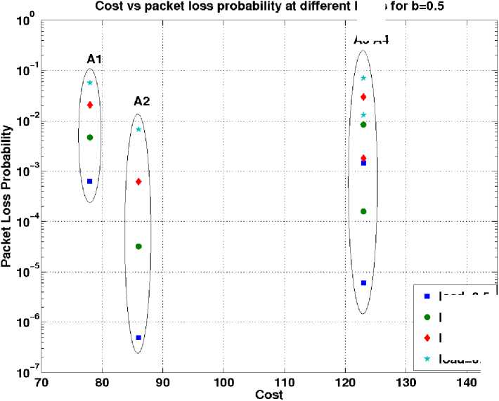
As we have discussed in the section 3 of the paper the complexity of the architecture A4 is highest while for architecture A2 it is lowest. Hence, the architecture A2 has inherent advantage in comparison to other architectures. The another important criterion for the switch performance is the packet loss probability. It is found from Figure 7 that the packet loss probability of the architecture A2 is lowest. In all, we are looking for a switch with lesser packet loss probability and comparatively lesser in cost. The cost vs packet loss probability curve for switch architectures using FCC model is shown in Figure 10. Under the acceptable packet loss probability i.e.≤10-4 the architectures A1 and A3 are ruled out while the performance of architecture A2 is better in comparison to other architectures.
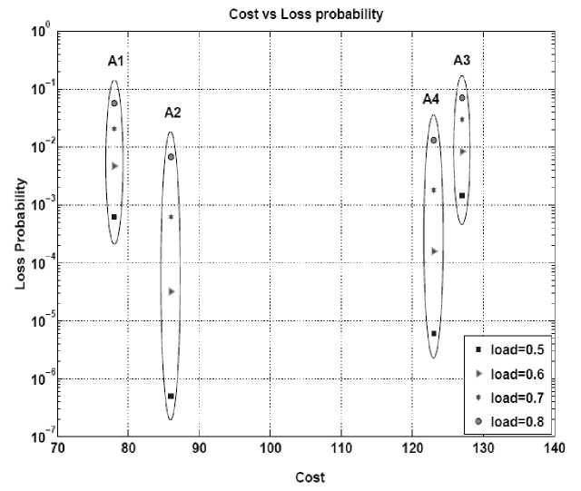
Fig 10: Cost vs. Packet loss Probability using FCC
loads
АЗ А4
load=0.6
load=0.7
Fig. 11: Cost vs. Packet loss Probability using WSU for b=0.9
load=0.5
load=0.8
In case of the WSU model (Figure 11 - Figure13) the architectures A1 and A3 do not provide acceptable packet loss probability. However as wavelength speedup characterization parameter (b) increases the cost increases but still the cost of A2 is lesser in comparison to architecture A4. Hence, it can be concluded that the architecture A2 outperform other architectures in terms of functionality, packet loss probability and optical cost.
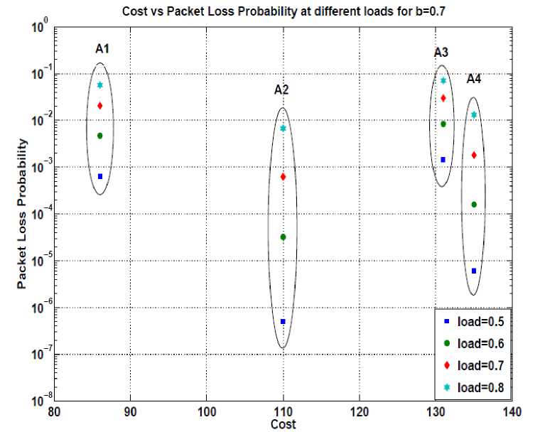
Fig 12: Cost vs. Packet loss Probability using WSU for b=0.7
Cost vs Packet loss at different loads for b=0.9
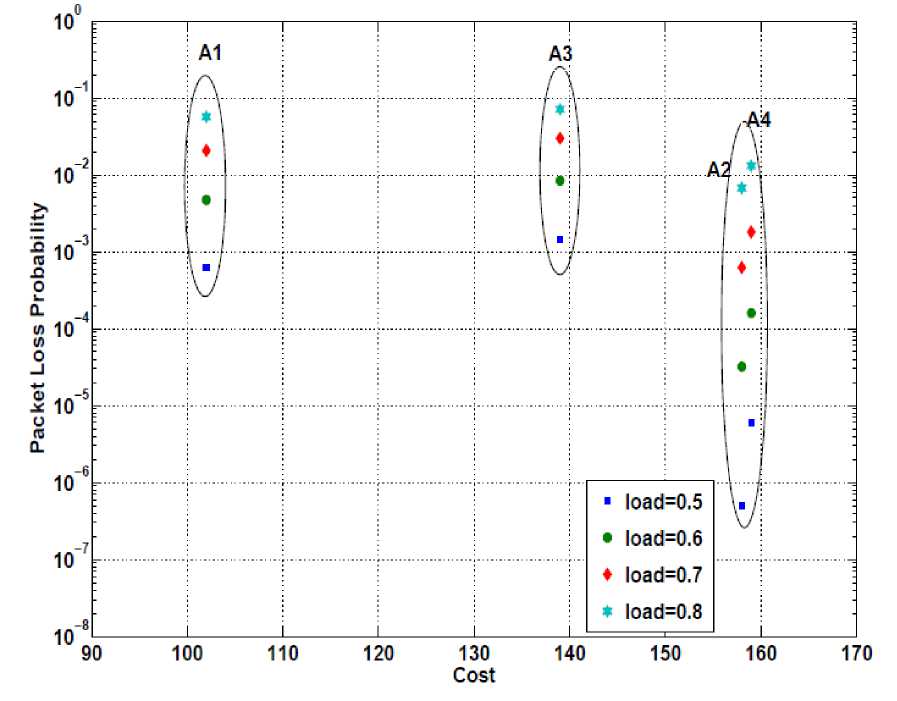
Fig. 13: Cost vs. Packet loss Probability using WSU for b=0.9
References Optical Packet Switch Architectures: A Comparative Study
- R. S. Tucker and W. D. Zhong, “Photonic packet switching: An overview,” IEICE Trans. Electron., Vol. E82-C, pp. 201-212, 1999.
- S. V. Kartalopoulos,"Introduction to DWDM Technology "(IEEE, 2000).
- Y. Shun, B. Mukherjee, S. J. B. Yoo, and S. Dixit, “A unified study of contention resolution schemes in optical packet switched networks,” J. Lightwave Technol. 21, 672683 (2003).
- E. F. Burmeister, D. J. Blumenthal, and J. E. Brown, "A comparison of optical buffering technologies,” J. Opt. Switch. Netw., vol. 5, no. 1, pp. 1018, Mar. 2008.
- D. K. Hunter, M. C. Chia, and I. Andonovic, “Buffering in optical packet switches,” J. Lightwave Technol. 16, 20812094 (1998).
- R. K. Singh and Y. N. Singh, “An overview of photonic packet switching architectures,” IETE Tech. Rev. 23, 1534 (2006).
- G. Bendelli, M. Burzio, P. Gambini, and M. Puleo, “Performance assessment of a photonic ATM switch based on a wavelength-controlled fiber loop buffer,” in Proceedings of IEEE Conference of Optical Fiber Communication (IEEE, 1996), pp. 106107
- N. Verma, R. Srivastava, and Y. N. Singh, “Novel design modification proposal for all optical fiber loop buffer switch,” in International Conference on Optoelectronics, Fiber Optics and Photonics (Photonics 2002), (Tata Institute of Fundamental Research, 2002), p. 181.
- R. Srivastava, R. K. Singh, and Y. N. Singh, “A modified photonic switch architecture based on fiber loop memory,” in Proceedings of IEEE Annual India Conference (IEEE, 2006), pp. 15.
- Y. Shun, B. Mukherjee, S. J. B. Yoo, and S. Dixit, “A unified study of contention resolution schemes in optical packet switched networks,” J. Lightwave Technol. 21, 672683 (2003
- D. J. Blumenthal, P. R. Prucnal, and J. R. Sauer, “Photonic packet switches: architecture and experimental implementations,” in Proc. IEEE 82, 16501667 (1994).
- F. S. Choa, X. Zhao, X. Yu, J. Lin, J. P. Zhang, Y. Gu, G. Piu, G. Zhang, L. Li, H. Xiang, H. Hadimioglu, and H. J. Chao, “An optical packet switch based on WDM technologies,” J. Lightwave Technol. 23, 9941013 (2005).
- Y. N. Singh, A. Kushwaha, and S. K. Bose, “Exact and approximate modeling of an FLBM-based all optical packet switch,” J. Lightwave Technol. 21, 719726 (2003).
- Z. Haas, "The staggering switch: an electronically controlled optical packet switches," J. Lightwave Technol. 11, 925936 (1993).
- R.Ramaswami, K.N., Sivarajan, “Optical Networks, A Practical Perspective,” 2nd ed. Morgan Kaufmann Publishers, 2002.
- R. Srivastava, R. K. Singh and Y. N. Singh, “WDM based optical packet switch architectures,” OSA J. Optical Netw., Vol. 7, No. 1, pp. 94-105, 2008.
- A. Frazen, D. K. Hunter, and I. Andonovic, “Synchronization in optical packet switch networks,” in Proc. Workshop All-Optical Network (WAON98), Zagrep, Crotia, May 1998.
- S. Shukla, R.Srivastava and Y. N. Singh, “Modelling of fiber loop buffer switch,” Proc. Photonics Conf., pp. 248, December, 2004.
- S. L. Danielsen, B. Mikkelsen, C. Joergensen, T. Durhuus and K. E. Stubkjaer, “WDM packet switch architecture and analysis of the influence of tuneable wavelength converters on the performance,” J. Lightw. Technol., Vol. 15, No. 2, pp. 219-226, 1997.
- R. V. Caenegem, D. Colle, M. Pickavet, P. Demeester, J. M. Martinez, F. Ramos and J. Marti, “From IP over WDM to all-optical packet switching:economical view,” J. Lightw. Technol., Vol. 24, No. 4, pp. 1638-1645, 2006.
- H. Li. and I. Li-Jin, “Cost-saving two layer wavelength conversion in optical switching network,” J. Lightw. Technol., Vol. 24, No. 2, pp. 705-712, 2006.
- Eramo and M. Listanti, “Packet loss in a bufferless optical WDM switch employing shared tunable wavelength converters,” J. Lightw. Technol., Vol. 18, No. 12, pp. 1818- 1833, 2000.
- R. Srivastava and Y. N. Singh, “Feedback fiber delay lines and AWG based optical packet switch architecture,” Opt.Switching Netw. 7 (2010) 75-84.
