Optimal Realization of Universality of Peres Gate Using Explicit Interaction of Cells in Quantum Dot Cellular Automata Nanotechnology

Author: Bisma Bilal, Suhaib Ahmed, Vipan Kakkar
Journal: International Journal of Intelligent Systems and Applications(IJISA) @ijisa
Article in issue: 6 vol.9, 2017.
Free access
The essence of the technology business lies in the improvements and advancements that are continuously taking place in the industry. From vacuum tubes, diodes and transistors to the concepts of nano level designing have by and large created a revolution in the history of mankind. The biggest milestone in this journey has been the CMOS technology which has managed to survive for decades and is still an ongoing research area. However, advancing the technology includes many other dimensions which need to be taken care of. As the devices go on decreasing in size with the improving technology the power dissipation in them becomes a major issue. To counter this, a new logic called reversible logic has come into the pool of research. Further a shift from the transistor based paradigm is being explored to go down to ultra-small structures. A major breakthrough in this can be the Quantum Dot Cellular Automata (QCA) Nanotechnology. In this paper we have given a review about how the reversible logic and QCA nanotechnology together result in ultra-low power designs. Further we have optimized the design of Peres reversible gate using the concepts of explicit interaction of cells in QCA and verified the universal functionality using the optimized designs.
QCA, Peres gate, universal gate, quantum dots, reversible computing, nanotechnology, circuit design, clocking
Short address: https://sciup.org/15010942
IDR: 15010942
Text of the scientific article Optimal Realization of Universality of Peres Gate Using Explicit Interaction of Cells in Quantum Dot Cellular Automata Nanotechnology
Published Online June 2017 in MECS
The success that has been achieved in miniaturization of the electronic devices is the result of downscaling of the basic MOSFET structure. The scaling includes the size retrenching along with the decrease in supply and threshold voltages. As the dimensions and parameters decrease, the removal of the dissipated power becomes more and more difficult. For this reason the power dissipation in the sub-micron technology regime has been an ever increasing concern for the researchers and designers [1-6]. In order to counter this issue a number of options are being suggested and explored. One of the most appealing among them is the reversible logic. This logic suggests a zero power dissipation in an ideal case. According to Landauer [10] the power that is dissipated in the digital circuits is not because of the processing of the bits that takes place within the device but due to the erasing of the bits that occurs in order to obtain the desired output. According to him erasing one bit of information results in a loss of KTln2 joules of energy where K is the Boltzmann’s constant and T is the temperature in Kelvin. Bennett [11] in 1973 showed that if the computations are performed in a reversible manner this KTln2 joules of energy loss can be avoided. For this to be achieved the circuits need to be designed using reversible gates and elements.
Reversibility is a phenomena in which there occurs a one to one mapping between the inputs and the outputs. This means that the inputs can be retrieved anytime form the output. Here each input corresponds to one particular output. In other words we can say that two rules need to be satisfied by a circuit or a gate to be called as reversible. First is the one to one mapping between the inputs and the outputs and the other is the equal number of inputs and outputs. If reversibility for a circuit is satisfied the power dissipation reduces to a great extent. The reversible logic and reversible circuits find applications in the field of quantum computing and low power design circuits. The optimization parameters in the case of reversible logic include the number of gates which overall determines the quantum cost of the circuits, the number of constant inputs that are used in realizing the function, the number of garbage outputs which are the unused outputs incorporated to satisfy the conditions of reversibility and the cost of the circuit which is the number of basic reversible elements used in the designing of the particular circuit. A number of reversible gates have been proposed in literature from time to time [1216], each having some functionalities and an improvement in the various optimization parameters. The realization of these reversible circuits has however been the greatest challenge faced by the researchers. Various reversible gates in literature are presented in table 1.
-
II. QCA Architecture
Ever since the scaling has taken the devices to nano level, the limitations of CMOS technology have been felt time and again. In the nano regime, the classical laws are no longer appropriate and various quantum mechanical effects start dominating. To counter this issue a number has emerged in the design of architectures is using nano of alternatives to replace CMOS are widely being sized structures like quantum dots [7-9].
researched. One of the most promising alternative that
Table 1. Various Reversible Logic Designs
|
S.No. |
Proposed Gates |
Gate Size |
Input Vector |
Output Vector |
OUTPUT |
|||
|
P |
Q |
R |
S |
|||||
|
1 |
Feynman Gate[12] |
2*2 |
I (A ,B ) |
0 (P ,Q ) |
A |
A ©B |
- |
- |
|
2 |
Double Feynman Gate[13] |
3*3 |
I (A ,B,C) |
0 (P, Q ,R) |
A |
A ©B |
A © C |
- |
|
3 |
Toffoli Gate [14] |
3*3 |
I (A ,B,C) |
0 (P, Q ,R) |
A |
В |
AB © C |
- |
|
4 |
Fredkin Gate[15] |
3*3 |
I (A ,B,C) |
0 (P, Q ,R) |
A |
A 'B ©AC |
A ' C ©AB |
- |
|
5 |
Peres Gate[16] |
3*3 |
I (A ,B,C) |
0 (P, Q ,R) |
A |
A ©B |
AB ©C |
- |
|
6 |
HAS Gate[33] |
3*3 |
I (A ,B,C) |
0 (P, Q ,R) |
A |
A ©B © C |
AB ©A'C |
- |
|
7 |
R Gate [36 ] |
3*3 |
I (A ,B,C) |
0 (P, Q ,R) |
A ©B |
A |
C'©AB |
- |
|
8 |
New Gate [35] |
3*3 |
I (A ,B,C) |
0 (P , Q ,R) |
A |
AB ©C |
A'C'©B' |
- |
|
9 |
TR Gate [41 ] |
3*3 |
I (A ,B,O |
0 (P , Q ,R) |
A |
A ©B |
AB ©)C |
- |
|
10 |
HNG Gate [17] |
4*4 |
I (A ,B,C,D ) |
0 (P ,Q ,R ,S) |
A |
В |
A©B©C |
(A ® B)C©AB©D |
|
11 |
HNFG Gate[18] |
4*4 |
I (A ,B,C,D ) |
0 (P ,Q ,R ,S) |
A |
A © C |
B |
B©D |
|
12 |
Multifunction Reversible Logic Gate [32] |
4*4 |
I (A ,B,C,D ) |
0 (P ,Q ,R ,S) |
A |
AB ©A ' C |
B^AC |
B©AC©D |
|
13 |
FAS Gate[33] |
4*4 |
I (A ,B,C,D ) |
0 (P ,Q ,R ,S) |
A ©B© C |
(B© C©D)A ©(C©D)B |
C |
B©C©D |
|
14 |
BVF Gate [40] |
4*4 |
I (A ,B,C,D ) |
0 (P ,Q ,R ,S) |
A |
A ©B |
C |
C©D |
|
15 |
TSG [37] |
4*4 |
I (A ,B,C,D ) |
0 (P ,Q ,R ,S) |
A |
A 'C'©B' |
(A'C'©B’ ' )©D |
(A ' C ' ©B ' )©D©(AB©C) |
|
16 |
PFAG[39 ] |
4*4 |
I (A ,B,C,D ) |
0 (P ,Q ,R ,S) |
A |
A ©B |
A©B©C |
(A©B)C©AB©D |
|
17 |
RAM Gate[38] |
4*4 |
I (A ,B,C,D ) |
0 (P ,Q ,R ,S) |
A |
A ©B |
A©B©C |
A©B©C©D |
|
18 |
MKG [ 34] |
4*4 |
I (A ,B,C,D ) |
0 (P ,Q ,R ,S) |
A |
C |
(A'D'©B'^©C |
(A'D'©B')C©(AB©D) |
QCA, developed by C.S. Lent in 1993, is a cellular automata type architecture as suggested by Von Neumann. The basic design cell in QCA consists of four nano sized quantum dots or metal islands in which two electrons are allowed to localize. The quantum dots/metal islands are separated by tunnel junctions. This is shown in fig 1.
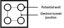
Fig.1. Basic QCA Cell
The basic principle of working is the quantum mechanical tunneling and coulombic interactions. The quantum mechanical tunneling is governed by the Schrodinger’s equation which leads to the lowering and raising of the barriers between the potential wells like the quantum dots. The electrons which are present in the dots can move from one dot to another only when the tunnel junctions between the dots are open otherwise they are trapped inside a particular quantum dot or the metal island whatever the case may be. Since the cell is a square structure with four quantum dots and two electrons, the coulombic repulsions between the electrons allow for only two type of stable configurations which are called as the two polarizations of the cell. They represent the binary zero and binary one depending on the position of the electrons in the dots. This is shown in the fig. 2.
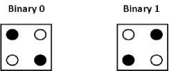
Fig.2. Two possible alignments of electrons in a QCA cell
Digital circuits and architectures can be designed using the basic building blocks in Quantum Dot Cellular Automata (QCA). QCA follows the phenomenon of processing in wire and memory in motion which means that unlike the CMOS and other technologies interconnections are not different from the general design. The interconnections have been a major issue in nano ranges since the interconnections do not scale with the scaling of other parameters. The basic building blocks in QCA include the binary wire, the inverter and the majority voter. In the case of the binary wire, shown in fig. 3, the polarization of a cell has the effect on the polarization of the adjacent cells. The cells take up the polarization of the input cell in order to settle for the most stable state. This state is then propagated from one cell to another.
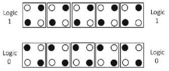
Fig.3. Binary Wire
In the case of the inverter the corner cell is placed at 45 ° with respect to the adjacent cell. Due to this configuration the corner cells takes up the opposite polarization to achieve a stable state with minimum coulombic repulsion. This is shown in fig. 4.
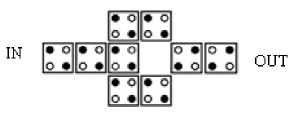
Fig.4. Inverter
The majority voter is the most important building block in QCA. It implements the equation A В + В С + А С . As shown in the fig. 5 the central cell in the majority voter is called as the device cell and it takes up the polarization of majority of inputs, that is why the name. This is because that state forms the ground state for the device cell.
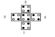
Fig.5. Majority Voter
The individual cells in QCA can have the effect of their polarization only up to a certain distance called as the radius of effect. Beyond that distance the effect of the polarization of the cell ceases to exist. For the proper flow of information in QCA circuits, they are provided with clock signals. The clock signals are responsible for raising and lowering of barriers and therefore controlling the polarization of the cells. The clock has four phases, shown in fig. 6. During the switch phase the barriers are lowered and the cells are allowed to take up a particular polarization depending on the polarization of the adjacent cells. This phase is followed by the hold phase in which the barriers are held high and the cell now effects the polarization of the adjacent cells and its own polarization remains unchanged. Release and relax phases are the next to follow which again lower the barriers and bring the cell back to the null polarization state. Four clocking zones are provided to QCA for proper pipelining of the information. The different clock zones in QCA are represented by different colors e.g. clock zone 0 is represented by green, clock zone 1 by magenta, clock zone 2 by blue and clock zone 3 by white.
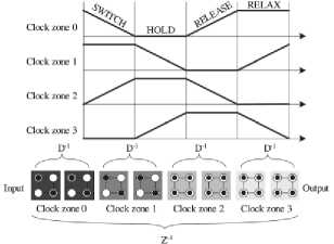
Fig.6. Different Clock Phases and Zones in QCA
-
III. Proposed Peres Gate Design in QCA
Designing new reversible gates and circuits has always been a focus for researchers since the field of reversible computing has made its way into the design of architectures [17-23]. The design of these gates in QCA has been a more recent trend in order to investigate QCA as a breakthrough for the realization of such gates. Conventional design approaches have been used as of now for designing the reversible structures. However some basic gates which have been proposed can be explored and optimized by using new design approaches other than the conventional majority voter designs. This is what has been aimed in this paper.
Peres gate is a 3*3 reversible gate which has the advantage of being used as a universal reversible gate. It can thus be used to implement all the basic Boolean functions. The gate has three inputs I (A,B , C) and three outputs 0 (P,Q,R ) . The outputs have been defined as P = A; Q = A фВ; R = AB ф C . Fig. 7 shows the block diagram and quantum representation of the Peres gate.
A
B
C
Peres Gate
P = A
Q = A ⊕ B
R = AB ⊕ C
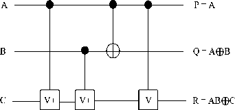
Fig.7. Peres Gate and its Quantum Implementation
The reversibility of the Peres gate is verified using the truth table as shown in table 2. A number of designs of Peres gate in QCA have been implemented from time to time [24, 25, and 27]. However the design parameters in them are not very efficient such as the cell count, is very large in these designs.
Table 2. Truth Table of Peres Gate
|
A |
B |
C |
P |
Q |
R |
|
0 |
0 |
0 |
0 |
0 |
0 |
|
0 |
0 |
1 |
0 |
0 |
1 |
|
0 |
1 |
0 |
0 |
1 |
0 |
|
0 |
1 |
1 |
0 |
1 |
1 |
|
1 |
0 |
0 |
1 |
1 |
0 |
|
1 |
0 |
1 |
1 |
1 |
1 |
|
1 |
1 |
0 |
1 |
0 |
1 |
|
1 |
1 |
1 |
1 |
0 |
0 |
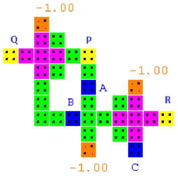
In our proposed design the explicit interaction of cells approach is used to reduce the cell count in our designs [26]. This approach of explicit interaction of cells suggests the impact of the polarization of cells on each other can actually make the array of cells to behave in a particular manner. Fig. 8 shows the QCA implementation of proposed reversible Peres gate along with the simulation waveforms in QCA designer 2.0.3.
For clearly demarcating the output we have shown the desired outputs in rectangular outline. The waveform in the highlighted rectangles are in correct coordination with the truth table of the Peres gate. This shows that our design and simulations are correct and optimized QCA design of reversible Peres can be achieved. This design of Peres gate marks a change from the conventional majority voter approach which involves the use of a larger number of cells and hence less optimized circuits.
On comparison with other designs, given in table 3, we can see that our designs are highly optimized in terms of all the parameters i.e. cell count, cell area, total area, latency and complexity. Besides no crossovers have been used in order to avoid the unnecessary complexity of the designs.
-
IV. Universality of Peres Gate
A gate can be called as universal if it can implement all the basic functions like the OR, NOR, AND, NAND, EX-OR, EX-NOR, NOT. The universality of Peres gate has been validated and all these functions have been realized using the Peres gate by manipulating the constant and other inputs. Besides it’s also seen that the number of garbage outputs remains minimum in the designs. Table 4 shows the manipulation of the inputs to achieve the desired functions at the output.
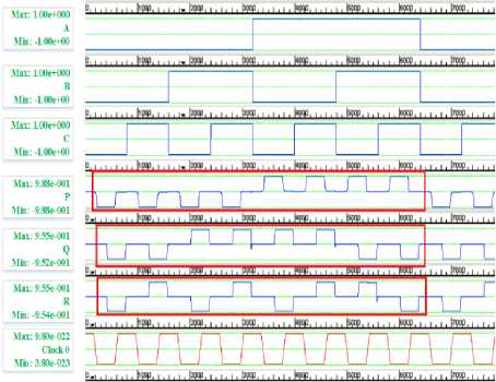
Fig.8. QCA implementation and simulation results of Peres gate in QCA Designer 2.0.3
Table 4. Basic gate functions obtained using Peres gate
|
S. No. |
Circuit |
Peres Gate Function |
|
1 |
NOT Gate |
Peres (A,1,1) |
|
2 |
AND Gate |
Peres(A,B,0) |
|
3 |
NAND Gate |
Peres(A,B,1) |
|
4 |
OR Gate |
Peres(A’,B’,1) |
|
5 |
NOR Gate |
Peres(A’,B’,0) |
|
6 |
Ex-OR Gate |
Peres(A,1,C) |
|
7 |
Ex-NOR Gate |
Peres(A,1,C’) |
The QCA implementations of the various logic gates designed with Peres Gate are discussed next.
-
A. NOT Gate
The NOT Gate is the most basic and important gate in the digital circuits. It performs the inverting operation and finds application in various digital circuits and electronic functions. Here Peres gate is used to design an inverter circuit. This is done as the first implementation to show the universality of the Peres reversible gate. The NOT
Table 3. Comparison of various Peres gates
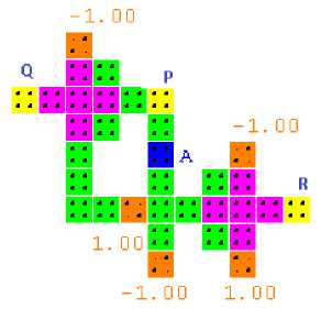
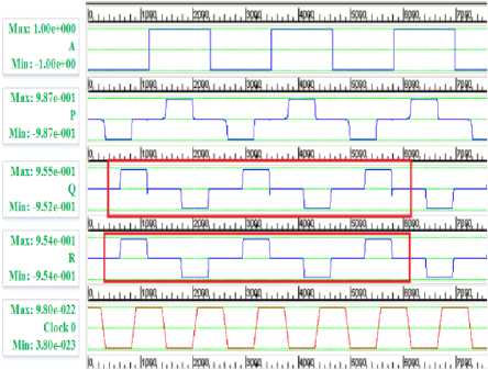
Fig.9. NOT Gate and simulation waveform
-
B. AND Gate
The AND operation is used in digital circuits and arithmetic whenever the product of two signals is needed as the output. Using the Peres gate the AND function can be realized by setting the third input C to a constant polarization of -1.00 as shown in Fig. 10. Due to this constant value the gate performs a logical AND on the two input signals.
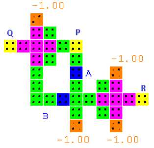
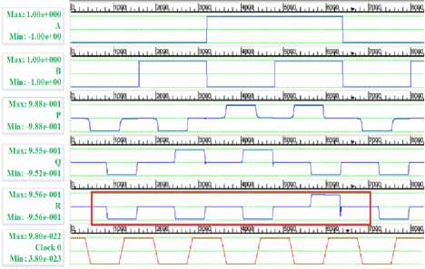
Fig.10. AND Gate and simulation waveform
-
C. NAND Gate
The NAND operation is achieved by setting the third input to a constant polarization of 1.00 as shown in Fig. 11. Due to this polarization the explicit interaction of cells causes the effect of cells on adjacent cells to realize the logical NAND operation.
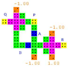
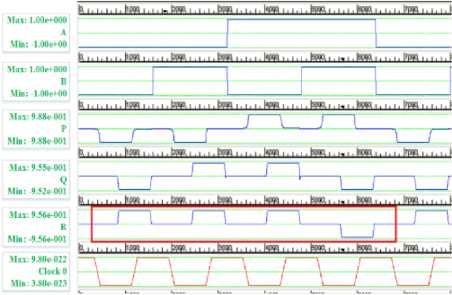
Fig.11. NAND Gate and simulation waveform
-
D. OR Gate
The OR operation is another basic function which should be realized by a particular gate to call it a universal gate. The OR operation is one of the most important operation in the digital circuits and forms the main operation in the multiplexing functions. Here the Peres gate is used to implement the OR operation by fixing the third input to a constant polarization of 1.00 and providing inverted signals at the first two inputs. The circuit is simulated in QCA Designer 2.0.3 and the waveforms achieved are shown in the Fig. 12. The delay that is obtained due to the clocking of the circuits is incorporated into the output, hence the correct output is shown by a rectangular box outline.
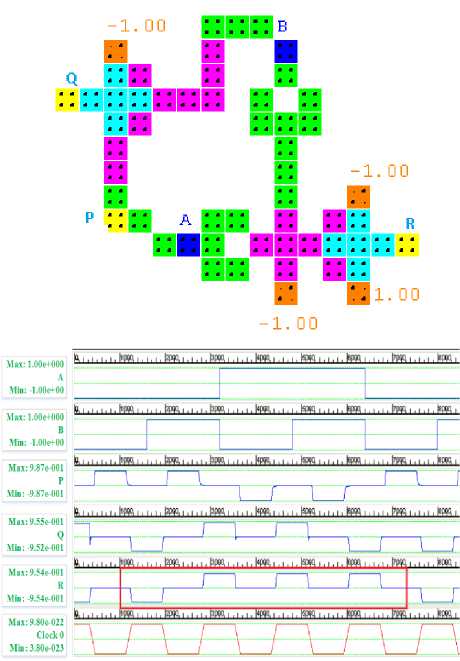
Fig.12. OR Gate and simulation waveform
E. NOR Gate
An inverted OR function is called as a NOR function. In the case of the Peres reversible gate, this is achieved by providing inverted waveforms at the first two inputs and a fixed polarization of 1.00 at the third input, as shown in Fig. 13.
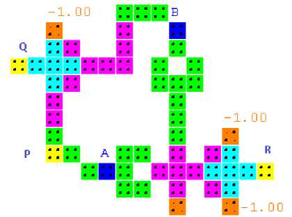
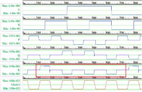
Fig.13. NOR Gate and simulation waveform
F. Ex-OR Gate
The exclusive OR function, also called as the controlled not circuit has a wide applicability in the digital circuits where controlled operations are required. Here Peres gate is shown to successfully achieve the Ex-OR function by maintaining a constant polarization of 1.00 at the second input. Since the second input now is one, the third output which is AB ⨁ С is changed to д⨁ с which is in fact the realization of an exclusive OR operation. This is shown in the Fig. 14.
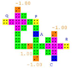
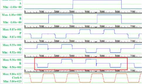
Fig.14. Ex-OR Gate and simulation waveform
G. Ex-NOR Gate
An inverted ex-or performs a logical Ex-NOR operation and is achieved in Peres gate by setting the second input to a constant polarization of 1.00 and supplying an inverted signal at the third input as shown in Fig. 15.
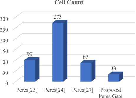
Fig.16. Comparative figures of Cell Count of Peres
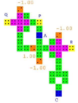
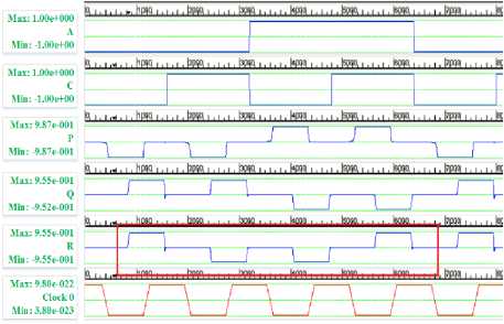
Fig.15. Ex-NOR Gate and simulation waveform
Latency (in clock cycles)
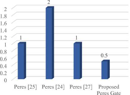
Fig.17. Comparative figures of Latency of Peres gate
-
V. Discussion
The proposed implementation of Peres gate using explicit interaction of cells in QCA has been compared with some of the recently reported implementations of Peres and the comparison results are presented in figures 16-19. It is observed that the proposed Pere gate fulfills its functionality while achieving much better results in terms of cell count, latency, cell area and latency and is hence an optimized design for further applications.
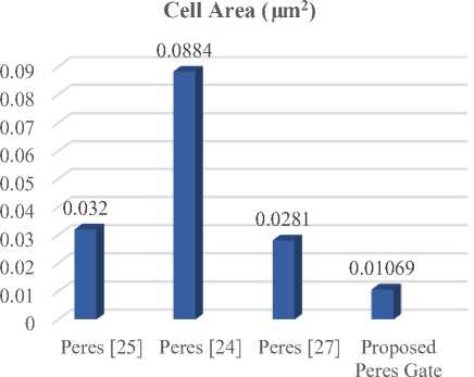
Fig.18. Comparative figures of Cell Area of Peres Gate
Total Area (µm2)
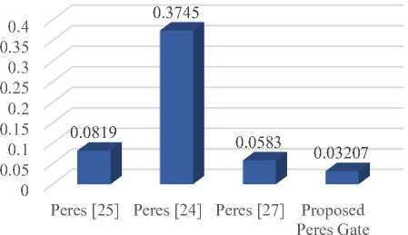
Fig.19. Comparative figures of Total Area of Peres Gate
The percentage performance comparison of the proposed optimized Peres gate design in QCA with other proposed designs is also presented in table 5, where each value depicts the percentage improvement of the performance parameter of the proposed Peres gate design with the already reported designs.
Table 5. Percentage Improvement of Proposed Peres Gate
References Optimal Realization of Universality of Peres Gate Using Explicit Interaction of Cells in Quantum Dot Cellular Automata Nanotechnology
- Yong B. Kim, “Challenges for nanoscale MOSFETs and emerging nanoelectronics”, Transaction on Electrical and Electronic Materials, vol. 11, no. 3, pp. 93–105, 2010.
- J. Gautier, “Beyond CMOS: quantum devices”, Microelectronic Engineering, Volume 39, Issues 1–4, December 1997, pp. 263-272.
- David Bishop, “Nanotechnology and end of Moore’s law”, Bell Labs Technical Journal, vol. 10, no. 3, pp. 23 - 28, 2005.
- G.E. Moore,” Cramming More Components onto Integrated circuits”, Proceedings of the IEEE, vol. 86, no.1, pp. 8 –85.
- John M. Shalf, Robert Leland, “Computing beyond Moore's Law” Computer, Volume: 48, Issue: 12, pp. 14 - 23, 2015.
- H. Iwai, End of the scaling theory and Moore's law, Proc. of 16th IEEE International Workshop on Junction Technology, (2016) 1-4.
- C. Lent, P.D. Tougaw, W. Porod, G.H. Bernstein “Quantum Cellular Automata,” Nanotechnology, Vol. 4, pp. 49–57, 1993.
- Wolfgang porod, “Quantum-dot devices and quantum-dot cellular automata”, International Journal of Bifurcation and Chaos, Vol. 7, no. 10, pp. 1147-1175, 1997.
- P.D. Tougaw, C.S. Lent, “Logical devices implemented using quantum cellular automata”, Journal of Applied Physics , vol 75, no. 3, pp. 1818-1825,1994.
- R. Landauer,” Irreversibility and Heat Generation in the Computing Process”, IBM Journal of Research and Development, Vol 5, No. 3, pp. 183-191,1961
- C.H. Bennett , “Logical Reversibility of Computation”, IBM Journal of Research and Development, vol. 17, pp. 525-532, 1973
- R. Feynman, “Quantum Mechanical Computers,” Optical New, pp. 11- 20, 1985.
- B. Parhami, “Fault Tolerant Reversible Circuits,” Proc. 40th Asilomar Conf. Signals, Systems, and Computers, Pacific Grove, CA, pp.1-4, 2006
- T.Toffoli, “Reversible Computing,” Technical Report MITLCSTM151, MIT Laboratory for Computer Science, pp. 632-644, 1980.
- E. Fredkin, T. Toffoli, “Conservative Logic,” International Journal of Theoretical Physics, vol. 21, pp. 219–253, 1982.
- A. Peres, “Reversible Logic and Quantum Computers,” Physical review, vol. A 32, pp. 3266-3276, 1985.
- A. K. Biswas, M. M. Hasan, A. R. Chowdhury and H. M. H. Babu, “Efficient approaches for designing reversible Binary Coded Decimal adders,” Microelectronics Journal, vol. 39, pp. 1693-1703, 2008.
- M. Haghparast and K. A. Navi, “Novel reversible BCD adder for nanotechnology based systems,” American Journal of Applied Sciences, vol. 5, pp. 282-288, 2008.
- Darushini Kunalan, Chee Lee Cheong, Chien Fat Chau, Azrul Bin Ghazali ,”Design of a 4-bit Adder using Reversible Logic in Quantum-Dot Cellular Automata (QCA)”, IEEE International Conference on Semiconductor Electronics (ICSE), pp.60-63, 2014.
- Ali Newaz Bahar, Sajjad Waheed, Md. Ahsan Habib ,”A Novel Presentation of Reversible Logic Gate in Quantum dot Cellular Automata (QCA),” IEEE International Conference on Electrical Engineering and Information & Communication Technology (ICEEICT), pp. 1-6, 2014
- K.S Mahalakshmi, Shiva Hajeri, H V Jayashree, Vinod Kumar Agrawal, “Performance Estimation of Conventional and Reversible Logic Circuits using QCA Implementation Platform,” IEEE International Conference on Circuit, Power and Computing Technologies (ICCPCT), pp.1-9, 2016
- Manisha G. Waje, P.K. Dakhole,” Implementation and Performance analysis of single layered reversible Parity generator and Parity checker Circuits using Quantum Dot Cellular Automata paradigm”, IEEE International Conference on Control, Instrumentation, Communication and Computational Technologies (ICCICCT), pp.175-180, 2015
- Amir Mokhtar Chabi, Arman Roohi, Ronald F. DeMara, Shaahin Angizi, Keivan Navi, Hossein Khademolhosseini, “Cost-Efficient QCA Reversible Combinational Circuits Based on a New Reversible Gate”, IEEE 18th CSI International Symposium on Computer Architecture and Digital Systems (CADS), pp.1-6, 2015
- A. Shafi, M. Shifatul, A. Newaz, “A Review on reversible logic gates and its QCA implementation,” International Journal of Computer Applications, vol. 128, no.2, pp. 27-34, 2015.
- A. Sarker, “A novel presentation of Peres gate (PG) in quantum-dot cellular automata (QCA)”, Eur. Sci. J., vol. 10, no. 21, pp. 101-106, 2014.
- Firdous Ahmad, Ghulam Bhat, Hossein Khademol Hosseini, Saeid Azimi, Shaahin Angizi, Keivan Navi, “Towards single layer quantum-dot cellular automata adders based on explicit interaction of cells”, Journal of Computational Science , vol. 16, pp. 8–15, 2016.
- J. Iqbal Reshi, M. Tariq Banday, “Realization of Peres gate as universal structure using quantum Dot cellular automata,” Journal of Nanoscience and Technology, vol. 2, no. 2, pp. 115–118, 2016.
- R. Devadoss, K. Paul; M. Balakrishnan, “Coplanar QCA crossovers”, Electronics Letters, vol. 45, no. 24, pp. 1234 - 1235, 2009.
- M. M. Arjmand, Mohsen Soryani, Keivan Navi, “Coplanar wire crossing in quantum cellular automata using a ternary cell”, IET Circuits, Devices & Systems, vol. 7, no. 5, pp. 263 – 272, 2013
- Dariush Abedi, Ghassem Jaberipur, Milad Sangsefidi, “Coplanar full adder in quantum-dot cellular automata via clock-zone-based crossover”, IEEE transactions on nanotechnology, vol. 14, no. 3, 2015.
- R. Devadoss, K. Paul, M. Balakrishnan, “Clocking-Based Coplanar Wire Crossing Scheme for QCA”, 23rd IEEE International Conference on VLSI Design, pp. 339 – 344, 2010.
- Vinay Kumar, Divya Dhawan, “Design of Reversible Adder Subtractor Using Multifunction Reversible Logic Gate (MRLG)”, International Journal of Advances in Computer and Electronics Engineering, no. 2, pp. 5–11, 2016.
- Neeraj Kumar Misra, Subodh Wairya, V.K. Singh, “Frame of reversible BCD Adder and Carry Skip BCD Adder and Optimization using new reversible gates for Quantum Dot Cellular Automata”, Australian Journal of Basic and Applied Science, vol. 9, no.31, pp.286-298,2 015.
- Majid Haghparast, Keivan Navi,”A Novel Reversible Full Adder Circuit for Nanotechnology Based Systems”, Journal Of Applied Sciences, vol. 7, no. 24, pp.3995-4000, 2007.
- Majid Mohammadi, Mohammad Eshghi, Majid Haghparast, Abbas Bahrololoom, “Design and Optimization of Reversible BCD Adder/Subtractor Circuit for Quantum and Nanotechnology Based Systems”, World Applied Sciences Journal, vol. 4, no. 6, pp.787-792, 2008.
- V.Kamalakannan, Dr P.V.Rao, Veeresh Patil, “Analysis of Reversible Binary Adder/Subtractor Circuit”, International Journal of Advanced and Innovative Research, pp. 129-134, 2012.
- Himanshu Thapliyal, M.B Srinivas, “Novel Reversible TSG gate and its Applications for designing Reversible Carry Look Ahead Adder and other Adder Architectures”, Proc. of 10th Asia Pacific Computer Systems Architecture Conference (ACSAC), vol. 3740, Springer Verlag, pp. 775-786, 2005.
- H.G. Rangaraju, Aakash Babu Suresh, K.N. Muralidhara, “Design and Optimization of Reversible Multiplier Circuit”, International Journal of Computer Applications, vol. 52, no.10, pp. 44-50, 2012.
- M.S. Islam, M.M. Rahman, Z. Begum, M.Z. Hafiz, “Low cost quantum realization of reversible multiplier circuit”, Information Technology Journal, vol. 8, no. 2, pp.208-213, 2009,
- H.R. Bhagyalakshmi, M.K. Venkatesham, “An Improved Design of a Multiplier Using Reversible Logic Gates”, International Journal of Engineering Science and Technology, vol. 2, no. 8, pp. 3838-3845, 2010.
- Himanshu Thapliyal, Nagarajan Ranganathan, “Design of Efficient Reversible Binary Subtractors Based on A New Reversible Gate”, IEEE Computer Society Annual Symposium on VLSI, pp.229-234, 2009.
