Performance analysis of LT codec architecture using different processor templates

Author: S. M. Shamsul Alam
Journal: International Journal of Information Technology and Computer Science @ijitcs
Article in issue: 8 Vol. 11, 2019.
Free access
Luby Transform (LT) code plays a vital role in binary erasure channel. This paper portrays the design techniques for implementation of LT codec using application specific instruction set processor (ASIP) design tools. In ASIP design, a common approach to increase the performance of processors is to boost the number of concurrent operations. Therefore, optimizations like strategy of input design, processor and compiler architecture are very useful phenomenon to enhance the performance of the application specific processor. Using Tensilica and OpenRISC processor design tools, this paper shows the response of LT codec architectures in terms of cycle counts and simulating time. Result shows that, the simulation speed of Tensilica is very high compared to the OpenRisc tool. Among different configurations of Tensilica tool, proposed ConnXD2 design took 1 M cycles per second and 135.66 ms to execute LT codec processor and XRC_D2MR configuration consumed only 9 iterations for successful decoding of LT encoded signal. Besides this, OpenRisc tool took 142K cycles and 6ms for executing LT encoder.
Luby Transform Code, processor design tools, cycle count, Simulation Speed, Custom Architecture
Short address: https://sciup.org/15016380
IDR: 15016380 | DOI: 10.5815/ijitcs.2019.08.06
Text of the scientific article Performance analysis of LT codec architecture using different processor templates
Published Online August 2019 in MECS
Luby Transform (LT) code nowadays plays an important role in the area of fountain code. This paper reports the various techniques for implementation of LT codec using application specific instruction set processor (ASIP) design tools. In past few decades, researches had been carried out to dedicate the operation of processor on application specific domain. In past few years, processor architectures had been evolved in the area of RISC family. Some key concepts like instruction level parallelism (ILP), bypassing technique, and multiple instruction executions are included with the operation of the RISC processors. To build complex systems, designers can integrate the pre-designed and pre-verified intellectual property (IP) blocks to save the time to market of a product. Designers are working hard to meet the requirements of embedded system design constrains like enhanced performance, less area, low power and less time to market. These ASIP architectures can replace multiple chip designs implemented as ASIC architecture [2]. Based on the coverage of full functionality of input application, the main target of ASIP design is to gain the highest performance over silicon area and power consumption as well as the highest performance over design cost [1]. ASIP implementation is perfect for this trade off and it is capable for scalable operation in terms of performance per area and power consumption factors [3]. In ASIP, a custom function unit in specific processor architecture is a partly designed application specific system that is used to adjust to a custom design with minimum cost. Therefore, this platform based system design requires minimum design cost during the plugging a programmable IP on the platform. This paper shows the unique technique to design LT codec processor using Tensilica and OpenRisc templates.
-
II. Related Works
The main contribution of this paper is to design an efficient LT processor which is optimized in terms of instructions and implementing time. Therefore, it requires processor design tool that can be customised as per LT codec input application that is known as hardware modification. Moreover, besides the modification of processor architecture, it is also necessary to write an efficient LT codec program using high level language which is known as software implementation. Using Tensilica and OpenRISC tools, these hardware and software implementation of LT codec are designed in terms minimum instructions and low simulation time which are the main criterion of application specific processors. So, to design an efficient LT codec processor is the main aim of this paper.
There are various approaches of software implementation of LT codec program. Systematic decoding of LT encoder and decoder is one of the new approaches of LT codec architecture [11]. In this paper T. D. Nguyen et al. shows that this newly systematic approach is very much preventive against a potentially avalanche-like inter-packet error while decoding process. To achieve the reduced complexity of LT encoder and decoder, the activities of check node operation and variable node operation are very important [12]. H. Hussien et al. proposed an efficient hardware architecture to reduce the check node complexity that improves hardware implementation in terms of speed and area. This customised architecture is also strong against error propagation [12]. To implement of LT codec, degree distribution and random number generator are very important functions to measure the level of complexity. T. Nguyen et al. showed a new approach of an optimized degree distribution and random number generator for software implementation of LT codec [13]. This newly approach of degree distribution is known as Truncated Degree Distribution (TDD). In LT decoder, sign of loglikelihood ratio (LLR) is used in belief propagation (BP) decoder structure. C. Albayrak et al. proposes a method that has less computational complexity in terms of iterations for decoding LT encoded signal [14]. J. He et al. discussed regarding Distributed Luby transform (DLT) codec and analysed the error floor performance over additive white Gaussian noise (AWGN) channels [15]. K. Zhang et al. showed an architecture of LT decoder with a block length of 1024 bits and 100 iterations [16]. In this paper, number of iterations of BP algorithm in LT decoding is very high. Based on the discussion on recent works, new approach of degree distribution, ASIC implementation, and ideal random integer generator of LT codec had been proposed. But in my paper I have designed an application specific LT codec processor which is a new approach in this area.
The rest of this paper is organized as follows: Section III describes the design techniques of LT codec processor using different processor templates. In this paper, Tensilica and OpenRisc processor tools have studied and proposed processor of LT codec has been developed. This Section represents the basic theories for developing processors using these tools. By using these architectures, LT codec program has been simulated which is shown in section IV. This section shows these simulation results generated by these tools. Here mainly cycle counts and simulation time are taken as reference parameters for comparing the performance of the tools. After simulating using all these tools, then a comparison table is portrayed to get the overall scenario of these tools. Finally conclusion and future works are discussed in final section.
-
III. LT Codec Processor Design using ASIP Design Tools
In this paper, we will show the processor design techniques using Tensilica and OpenRISC tools. For application specific processor design, at first it requires two design files: one is input application written in HLL (for example in this work ltcodec.c file) and second one is processor architecture file (for example architecture definition file .adf, configuration file .cfg etc). These two design files are key structures for processor design in application specific domain. The response of the processor depends upon these input design files. For this reason, it is very important for designers to make efficient architecture of input application and configuration files. The proposed architecture of LT codec is discussed in author’s paper [4]. It is necessary one tool set for implementing application specific processors based on the TTA processor template. TTA based Co-Design environment (TCE) is one such processor template to provide an efficient LT codec processor written in high level language (HLL). This toolset is developed by Tampere University of Technology [5]. The comprehensive design of LT codec using TCE is elaborately explained in author’s another paper [6]. Using this tool, application written in high level language can be implemented in FPGA evaluation board through RTL design flow.
-
A. Processor Design Using Tensilica Tool
Tensilica is very popular in the area of customizable processor design. It was founded by former employees of Silicon valley and EDA companies like MIPS in 1997. Like TCE tool, Tensilica also develops application specific processor for use in synthesized chip design for embedded system. Under Tensilica, Xtensa Xplorer is processor IP architecture used to generate processor for input application.
At first, I will discuss an ASIP oriented design flow using Xtensa Xplorer (XX) integrated development environment (IDE) as the design framework under Tensilica tool [7]. Using the XX, it is possible to integrate software development, processor optimization and multiple-processor system-on chip (SoC) architecture into one common platform. From it, we can profile our input application code to identify the cycle consumed by the function used in input design.
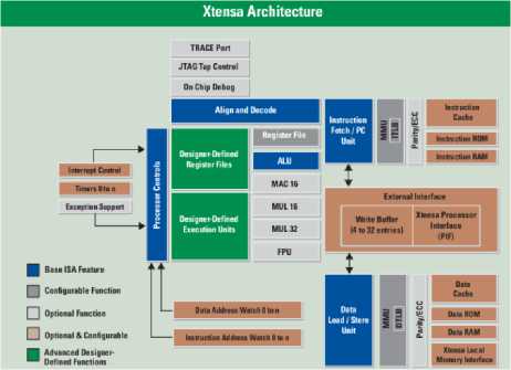
Fig.1. Configuration of Xtensa Xplorer Xtensa architecture [7]
Then we can make necessary change to speed up that code. There are various building blocks in the Xtensa architecture. The preconfigured cores are divided into four broad categories such as Communication, HiFi/Audio, Video/Imaging and Diamond or General Purpose Controller. Figure 1 shows the structure of Xtensa architecture. This figure shows the range of configurability, extensibility with Xtensa processor. In this architecture, system designer should specify the different blocks of configuration function units. Advanced designer-defined functions are one kind of hardware execution units and registers. Figure 2 represents overall design flow of XX [7]. In this figure, the first block contains different configurations selected upon the nature of input application. Based on these properties of this architecture, I have taken different configurations of architectures to simulate our input application. For this reason, I have taken 16 preconfigured cores and among them the result is tabulated for four Xtensa configurations. Then we apply some custom logic levels to processor for accelerating the processor performance.
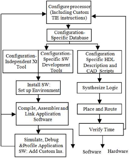
Fig.2. Configuration of Xtensa Xplorer Xtensa design Flow [7].
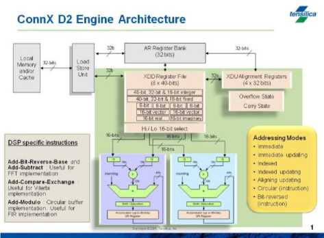
Fig.3. A simplified architecture of ConnXD2 DSP engine [8].
The Communication configuration core is known as ConnX D2 DSP engine. In this paper, two ConnX configurations known as XRC_D2MR and XRC_D2SA are used for simulation and show very good performance between all other configurations. The XRC_D2XX configuration includes dual 16-bit multiply-accumulate (MAC) units and 40-bit register file to the base RISC architecture of the Xtensa LX processor. This engine uses two-way SIMD (single instruction, multiple data) instructions to provide high performance on vectorizable C code. It implements an improved form of VLIW instructions and five-stage pipeline.
Figure 3 shows the basic architecture of the ConnX D2 engine with two MAC units with register banks [8]. The ConnX D2 instruction set is designed for numeric computations like add-subtract, add-compare or addmodulo etc required for digital signal processing.
This ConnX D2 core exploits seven DSP-centric addressing scheme mentioned in figure 3. In order to provide excellent performance, it includes data manipulation instructions like shifting, swapping, and logical operations. Our input design is LT codec and it has huge number of shifting, swapping and logical operations. So, this processor architecture is suitable for our input design[8]. Besides this, I have simulated our LT codec design using other configurations.
Tensilica Instruction Extension (TIE) is a language that lets designers incorporate application-specific functionality in the processor by adding new instructions. To accelerate the speed of the processor, in Tensilica, it is possible to apply the custom operation in input design. Tensilica Instruction Extension (TIE) language is a powerful way to optimize the processor and is used to describe new instructions, new registers and execution units that are automatically added to the Xtensa processor [8]. Xtensa cores take TIE files as input and create a version of Xtensa processor to complete the tool chain incorporate with new TIE instruction. The processor architect’s job is to decide which applications are common enough to warrant some level of support through dedicated instructions. This TIE can be generated automatically or manually, depends on the performance of TIE instructions. In this work, we have used TIE instructions generated automatically to profile our input design and it shows good performance. So using TIE instruction, processor creates single instructions that perform the multiple general purpose instruction. As mentioned above, TIE instructions improve the execution speed of the input application running on Xtensa processor. Some other techniques like Flexible Instruction Extensions (FLIX), Single Instruction Multiple Data (SIMD) and Fusion can be executable through TIE operation [8]. In this paper, we applied only FLIX instruction to the input application. In Xtensa, FLIX instructions are multi-operation instructions (32-bit or 64-bit long) that allow a processor to perform multiple, simultaneous, independent operations. In FLIX, processors are encoding the multiple operations into a wide instruction word. The XCC compiler takes the FLIX operation and converts it into FLIX format instruction as per the requirements to accelerate the input code. The performance of FLIX instruction is discussed in simulation result section.
-
B. Processor design using OpenRisc tool
The OpenRISC architecture is one of the latest in the development of modern open architectures. It consists a family of 32- and 64-bit RISC/DSP processors. This kind of architecture allows a spectrum of chip and system implementations at a variety of price/performance points for a range of applications. OpenRISC 1200 is a
synthesizable processor developed and managed by OpenCores and using this OR 1200 processor, systems are designed with emphasis on performance, simplicity, low power consumption, scalability, and versatility. It targets medium and high performance networking, portable, embedded, and automotive applications. Therefore, OR 1200 is an open source IP-core available from the OpenCores website as a Verilog HDL model. By using this tool, the design can be simulated by two ways. The first uses the RTL simulation of primary design by using Icarus Verilog or Mentor Graphic’s Modelsim and the second method involves creating a cycle accurate from hardware description language using verilator tool. In this paper, RTL simulation (Icarus Verilog Simulator) is done for reference designs by using OpenRisc architecture, which consists 5-stage singleissue integer pipeline, virtual memory support and basic DSP capabilities [10]. Figure 4 shows an overview of OpenRisc 1200 core architecture. For RTL implementation, all the blocks of OpenRisc 1200 IP core are written in Verilog HDL and are published under the GNU License. Here the test programs are compiled to Executable and Linkable Format (ELF) file format, which can be executed both in ISS and RTL simulator. Memory Addressing is one of the important operations of OpenRisc architecture. The processor computes an effective address when memory access instruction is executed. This addressing is also applicable for fetching the next sequential instruction. Fetching instructions from main memory is the main bottleneck of RISC processor. OpenRisc 1200 implements 32-bit 32 general-purpose registers (GPRs). The Load/Store Unit (LSU) transfers all data between the GPRs and CPU’s internal bus.
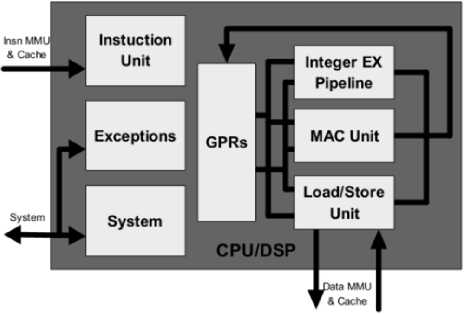
Fig.4. Architecture overview: CPU/DSP block diagram of OpenRisc [9]
Figure 4 shows the different units of CPU architecture in OpenRISC processor. The instruction unit implements the basic instruction sets of the OR1200 core. This instruction unit fetches instruction from the memory system and dispatches them to the available execution units like LSU, ALU, MAC units[9]. The basic operation of instruction unit is similar to that of the RISC processor. But The OpenRISC1000 architecture defines five instruction’s formats and two addressing modes those are explained elaborately in its product ref manual [9]. In figure 5, I have briefly explained these stages. Besides the
GPRs and SPRs, OR 1200 has some important registers like Supervision register, Exception supervision register, program counter register, exception program counter register and exception effective address registers.
OR 1200 has LSU which is responsible for transferring data between GPRs and the internal data bus of CPU. The LSU has been implemented as independent unit OR 1200 architecture so that if there is a data dependency then memory system only be affected. The LSU can execute one load instruction every two clock cycles. It has ALU like RISC processor architecture.
MAC unit executes the basic DSP operations and MAC instructions. In OR 1200 MAC unit is fully pipelined. In every clock cycle, it has ability to accept new MAC operation. The MAC instruction has 32-bit operands and a 48-bit accumulator. System unit connects all the CPU signals to the system signals except those which are connected through the Wishbone interfaces.The exception unit oversees the exceptions generated by the OR1200 processor core. For example the system calls, memory access conditions, interrupt request etc are handles by the exception units.
For this OpenRisc processor, there are five-stage pipeline named as fetch, decode, execution, memory and write-back as mentioned in figure 5. These five instructions are in progress at any given clock cycle and each stage of the pipeline performs its task in parallel with all other stages. So in this paper, the execution clock cycles are counted for OpenRisc processor by applying two reference designs named as LT encoder and LT decoder architectures. The result will be discussed elaborately in simulation result section.
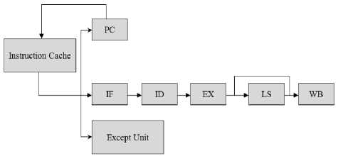
Fig.5. Architecture overview: OpenRISC 1200 5 stages pipeline.
Figure 5 shows the five stages pipeline architecture of OpenRISC processor. These stages are mentioned as instruction fetch (IF), instruction decode (ID), execute (EX), load store (LS), and write back (WB). Pipelining is one of the most important phenomenon to verify the processor. It has strong effort to speed up the processor. Using this pipelining technique an instruction’s execution is divided into a number of independent steps to improve the throughput of a processor. These independent steps are called pipeline stages. Each pipeline stage ends up in a storage (pipeline registers) of its execution so that the subsequent stages can use the result. Therefore the pipelining architecture of OR 1200 processor is similar to the pipelining that I have discussed elaborately in previous chapters.
In this section, I have discussed proposed architecture of LT codec, processor design using two different ASIP design tools and their architectures. Nevertheless, this discussion is not sufficient for understanding the complete tools. To get adequate information reference manual and user guides of corresponding tools are recommended. However, there are many other tools, for designing and simulating ASIP work. In this paper, I took only two tools for comparing their results.
-
IV. Simulation Result
I have implemented and generated application specific processor for LT codec using Xtensa and OpenRISC processor design tools. The simulation results of TCE tool set have been shown in author’s another paper in ref [6].
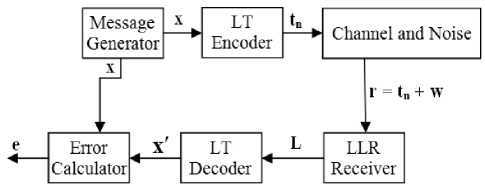
Fig.6. Simulation model of LT codec communication.
I have translated the complete encoding and decoding algorithm using C program. Before feeding in the decoding module, I apply noise to corrupt the transmitted signal through the channel. Therefore, the overall communication can be modeled by the figure 6. The main aim of this paper is to implement figure 6 using ASIP design tools. The results of this implementation based how efficiently I will produce LT codec processor and its efficiency is calculated in terms of cycle count and time required for simulation. Area, number of gates and cells required to implement this architecture have been discussed in reference [4].
-
A. Simulation Result Using Tensilica Tool
Now I am compiling the LTcodec input design as reference code along with its library for each of the sixteen target cores and then run a profile execution.
Table 1 represents the comparison of cycle counts for all processor configurations. As shown in table 1.1, the configuration components are designed according to the implementation of input design. From table 1.1, this processor is developed using TIE instruction set for LT codec input design and then add this TIE instruction with core processor named as XRC_D2SA.
Table 1. Comparison of cycle counts for different configurations of Tensilca tool
|
Active Processor Configuration |
Total cycles |
Required Time (s) |
|
DC_C_106micro |
229,213,917 |
163.71 |
|
DC_C_108mini |
219,797,553 |
171.82 |
|
DC_C_212GP |
204,964,527 |
164.23 |
|
DC_C_233L |
204,968,307 |
170.19 |
|
XRC_D2MR |
164,231,379 |
137.86 |
|
XRC_D2MR_FLIX |
162,629,766 |
135.66 |
|
XRC_D2SA |
208,465,165 |
157.37 |
|
XRC_D2SA_FLIX |
206,444,710 |
202.20 |
Now I am compiling the LTcodec input design as reference code along with its library for each of the sixteen target cores and then run a profile execution. Table 1 represents the comparison of cycle counts for eight processor configurations. As shown in table 1.1, the configuration components are designed according to the implementation of input design. Based on this, ConnXD2 category processor shows very good result compared to the other processor configurations. If we study the cycle consumed by different operations using Tensilica tool, there are huge addition and logical operations taken by the LT codec design. Due to this reason, ConnXD2 type processor is suitable for simulating this LT encoder and decoder. From table 1, We can see that, without custom instruction operation XRC_D2MR is the best in comparison to other processors. Moreover, in Diamond controller processor, 570T configuration outperforms compare to others. We see that, 570T processor contains many DSP instruction extensions and SIMD execution units. If we see the disassembly information of input function, it is easily possible to find the step-by-step cycle consumptions by main and children functions as per their configuration details. We are not going to discuss all these architectural analysis. As it is mentioned earlier that ConnX D2 architecture is suitable for communication and for its rich hardware resources, XRC_D2MR configuration without TIE or FLIX instruction, takes 164,231,379 total cycles for LT codec application. From its profile status, main function consumes highest 7,585,908 cycles and if we see the disassembly profile of main function, it takes many load, add, move and logical operations. So, when we think in terms of hardware, these operations are rewiring certain bits from input to output. For this reason, we develop TIE and FLIX instructions and include these custom instructions to the processor. Table 1 shows the result of eight target processor in terms of cycles. Significant improvement in terms of cycle counts was found and from this table, the XRC_D2MR_FLIX configuration took 162,629,766 cycles and main function took only 5,984,295 cycles which reduces 1,601,613 cycles compared to without FLIX operation. These architectures can be further modified by introducing the custom TIE instructions.
I have generated TIE instruction by using automatic TIE generation techniques as mentioned in section III. Now I will show the behavior of iteration vs cycle counts of LT codec implementation. It is mentioned earlier that the decoding complexities depend on the number of iterations required for recovering message from encoded signal. For XX it takes 9 iterations for successfully decoding the encoded signal. However, it is possible to reduce the number of required iterations by modifying the degree distribution in the encoder. Table 2 was simulated for fixed degree distributions using highest and lowest configurations. Therefore, number of cycles is increasing exponentially with respect to the number of iterations. So it is very important to trade off between several issues: degree distribution, architecture structure of processor configuration, architecture of LT encoder and decoder, and finally the status of binary erasure channel (BEC). Because, the value of failure probability (δ) depends on the characteristics of the channel and the average number of degree connected with variable node depends on the value of δ.
Table 1.1. Processor configuration of ltcodec_tie architecture
|
Configuration Overview |
|
|
User Name |
chosun_ice_edu/sub2 |
|
Core Name |
ltcodec_tie |
|
Core Description |
XRC_D2SA |
|
Configuration Detail |
|
|
TIE sources for configuration |
ltcodec.tdb contains ltcodec.tie |
|
Xtensa ISA version |
LX4.0 |
|
Instruction options |
|
|
16-bit MAC with 40 bit Accumulator |
no |
|
MUL 32 |
no |
|
32 bit integer divider |
no |
|
Single Precision FP |
no |
|
Double Precision FP Accelerator |
no |
|
Synchronize instruction |
no |
|
Conditional store synchronize instruction |
no |
|
MUL 16 |
yes |
|
CLAMPS |
yes |
|
NSA/NSAU |
yes |
|
MIN/MAX and MINU/MAXU |
yes |
|
SEXT |
yes |
|
Boolean Registers |
yes |
|
Number of Coprocessor(NCP) |
3 |
|
Enable Density Instruction |
yes |
|
Enable Processor ID |
yes |
|
Zero-overhead loop instruction |
yes |
|
TIE arbitrary byte enables |
yes |
For example, according to the table 2, for fixed value of δ, XRC_D2MR takes more that 340M cycles for 16 iterations on the other hand for diamond controller 106mico, it takes more than 475M cycles for 16 iterations. Moreover, simulating time behaves same as the manner of cycle counts.
Table 2. Simulation for different number of iteration using Tensilica tool
|
# of Iterations |
XRC_D2MR_MAC |
DC_C_106micro |
||
|
Cycle Count |
Time Count (s) |
Cycle Count |
Time Count (s) |
|
|
1 |
5,204,861 |
4.43 |
6,983,593 |
4.97 |
|
2 |
19,182,518 |
15.60 |
26,034,519 |
18.31 |
|
3 |
35,128,884 |
27.71 |
48,036,337 |
33.79 |
|
4 |
52,840,982 |
42.21 |
72,696,444 |
50.98 |
|
5 |
71,951,305 |
57.18 |
99,135,487 |
69.74 |
|
6 |
92,160,200 |
74.41 |
127,678,043 |
90.72 |
|
7 |
115,082,566 |
92.73 |
159,731,114 |
113.43 |
|
8 |
164,837,807 |
128.70 |
194,314,345 |
137.03 |
|
10 |
189,915,708 |
151.39 |
264,271,320 |
185.73 |
|
16 |
340,940,055 |
283.37 |
475,626,960 |
335.57 |
B. Simulation result using OpenRisc tool
For OpenRisc processor, “.cfg” file contains the default configurations and a set of simulation environments, which are similar to the actual hardware situation. For RTL simulator, the verilog files of all IP cores are included by using MAKE file. So once the environment is configured then the simulator generated the “.log” files under “out” and “run” folder. The minimal architecture of reference design is shown in table 3. In the OpenRisc processor, the reference design is compiled using OpenRisc tool chain (or32-elf) and a memory image is generated (.vmem). Then this program image is used in simulation to fill the RAM. Next, the verilog RTL sources check, compile, and simulate the result. Therefore, the OpenRISC processor will generate all the required signals to execute the operation.
Table 3. Simulation result by using OpenRisc processor encoder and decoder
|
OpenRISC Processor |
|||
|
Encoder |
Decoder |
||
|
cycle |
Time (ns) |
cycle |
Time (ns) |
|
142,015 |
6,174,570 |
153,353 |
6,712,850 |
In OpenRisc tool only modifying the CPU configuration is not sufficient to reduce the cycle count. For implementing the technique of sum product algorithm, it is required to use the sign function ( tanh or tanh-1 ) in LT decoding algorithm. Therefore, I modify the decoding architecture of LTcodec design as per requirements of OR C compiler by including the LUTs. But these LUTs are not efficient because of random number generator. For each new simulation this LUT should be changed due to change of RNG. But for implementing the LT encoder, it does not require any mathematical operation. So it is easily synthesized by OpenRisc core. However table 4 represents the simulation result using this processor.
There are some limitations for simulating LT codec design using OpenRisc processor. I successfully completed the implementation of encoder but in the decoding part implementation didn’t work properly. Due to the problem of header file, I mentioned earlier that
LUTs had been used there and these LUTs have been changed in each simulation because of random degree distribution. So it is not possible to calculate the error calculation of the LT codec. Since there is no option to transfer load from input design to compiler or simulator, so it is not possible to include the custom FU like TCE or custom instruction set like TIE and FLIX in OpenRisc processor. Only modification can be achievable by designing LTcodec architecture as input design or changing the CPU architecture of the processor. But the effect of changing CPU or simulation architecture shows very less impact on cycles count or simulation time. For this reason I didn’t represent the CPU architecture modification in this paper, although I have done this by changing setting the enable condition of different parameters under CPU section in reference configuration.
-
C. Comparison between LT codec processors
Now, it is necessary to mention that we already developed hierarchy of different architectures for LT codec by using Tensilica and OpenRisc tools. The comparison between Tensilica and OpenRisc will be displayed.
Table 4. Comparison of cycle counts for the Tensilica and OpenRISC processors
|
Tensilica |
OpenRISC |
||
|
Cyc. Cnt. |
Time(s) |
Cyc. Cnt. |
Time (ns) |
|
142,557 |
0.11 |
142,015 |
6,174,570 |
It is mentioned earlier that the TTA structure has more benefits compared to the OTA processor domain. In OTA domain, it takes separate instructions for executing the instructions using ISS environment. For this reason Xtensa tool takes more cycles for implementation. Tensilica runs 1 M cycles per second using ConnX D2 engine. Now to make a fair comparison with three tools I have simulated encoder part of LT codec by using these tools. Table VI shows this comparison result, which is responsible for getting the scenario of these three tools.
OpenRisc takes separate cycles for executing the instructions, which is a common behavior of the OTA class processor tools. However, all the architectures of these tools can be further modified by using their own techniques. Besides this, the modifications of LT codec i.e. degree distribution, number of decoding iteration, or input and encoded message length have huge influence on this hardware throughput. Within these three tools, Tensilica tool is very easy in terms of use and optimization. In this paper, I have used the Optimization level 3, automatic TIE and FLIX options of Tensilica tool. Moreover, the modification of configuration parameters of XX is not sufficient for designing the high performance LT codec design.
-
V. Conclusions
The step by step techniques of application specific processor design using Tensilica and OpenRISC tools have been discussed elaborately in the previous sections. Finally in the result, the comparisons of these tools are presented in different aspects.
OpenRISC tool is executing under the concept of pure pipelined RISC processor. On the other hand, XX of Tensilica shows the behavior like VLIW processor. As we discussed earlier that TTA is very suitable for applying custom FU to the architecture. Therefore, I have designed different custom FU for LT encoder and decoder. Similarly, in Tensilica tool, the processor configuration can be modified as per the input application in various ways. In this paper, TIE and FLIX technique are applied to improve the performance of processor in terms of cycle count. Finally the performance of the OpenRISC processor has been studied. I find some limitations while using the OpenRISC processor. For simulating the input design written in HLL, it does not support many of the header files. As a result, there should take some alternative solutions like LUTs or other functional program based on mathematical operations for generating the processor. However, the response of the processor are not solely depends on the processor architecture. This performance also depends on the input design architecture. Therefore, besides the designing of custom processor part, we need to design LT codec as a reference input efficiently. In this paper work, there are some observations I find during simulation time. There are many reconfigurable techniques for every tool. It is not possible to take all these optimization techniques. For example, I have used the Optimization level 3, automatic TIE and FLIX options for Tensilica tool. Moreover, the modification of configuration parameters of XX is not sufficient for designing the high performance LT codec design. Therefore, an efficient trade off is required between all these observations to satisfy an excellent processor based on the input application.
References Performance analysis of LT codec architecture using different processor templates
- D. Liu, “Embedded DSP Processor Design: Application Specific Instruction Set Processor,” M.K. Publishers, Elsevier, pp. 20-200, 2007.
- P. Radosavljevic, “Channel Equalization Algorithms for MIMO Downlink and ASIP Architectures,” Master’s Thesis, Rice University, Texas 2004.
- O. Esko, “ASIP Integration and Verification flow for FPGA,” Master’s Thesis, Tampere University of Technology, Tampare Finland, may 2011.
- S. Alam, and G. Choi, “Design and Implementation of LT Codec Architecture with Optimized Degree Distribution”, IEICE Electronics Express, Vol. 10, No. 12, doi: 10.1587/elex. 10.20130340, June 2013.
- TTA-based Co-design Environment v1.5. User Manual, Tampere University of Technology, Finland 2006.
- S. Alam, and G. Choi, “Design and Implementation of a Novel LT Codec Architecture on TTA Based Codesign Environment”, IEICE Electronics Express, Vol. 13, No. 13, pp.20160298, doi: elex.13.20160298, 2016.
- Tensilica Product, “Xtensa 7,” Product Brief.
- Tensilica Product, “ConnX D2 DSP Engine,” 2012 , http://www.tensilica.com/uploads/pdf/connx_d2_pb.pdf.
- D. Lampret, “OpenRISC 1000 Architecture Manual,” OpenCores (2012).
- K. Anantha Ganesh Karikar, “Automatic Verification of Microprocessor designs using Random Simulation,” Master’s thesis, Uppsala University, Sweden 2012.
- T. D. Nguyen, L. L. Yang, L. Hanzo, “Systematic Luby Transform Codes and Their Soft Decoding”, IEEE Workshop on Signal Processing Systems, doi: 10.1109/SIPS.2007.4387519, Chaina, 2007.
- H. Hussien, K.Shehata, S. Ramly, and N. Tawfik,” Design of a Merged Algorithm for Luby Transform Decoder”, International Journal of Computer and Communication Engineering, Vol. 1, No. 3, September 2012.
- T. D. Nguyen, L. L. Yang, S. X. Ng and L. Hanzo, “An Optimal Degree Distribution Design and a Conditional Random Integer Generator for the Systematic Luby Transform Coded Wireless Internet”, IEEE Wireless Communications and Networking Conference, DOI: 10.1109/WCNC.2008.48, USA, 2008.
- C. Albayrak, C. Sımsek, K. Türk, “Sign alterations of LLR values based early termination method for LT BP decoder”, 25th Signal Processing and Communications Applications Conference (SIU), doi: 10.1109/SIU.2017.7960434, Turkey, 2017.
- J. He, I. Hussain, Y. Li, M. Juntti, and T. Matsumoto, “Distributed LT Codes With Improved Error Floor Performance”, IEEE Access, doi: 10.1109/ACCESS.2018.2890452, Vol. 7, 2019.
- K. Zhang, X. Huang, and Chen Shen, “Soft decoder architecture of LT codes”, IEEE Workshop on Signal Processing Systems, doi:10.1109/SIPS.2008.4671764, 2008.
