Performance Analysis of Various Readout Circuits for Monitoring Quality of Water Using Analog Integrated Circuits

Author: Pawan Whig, Syed Naseem Ahmad
Journal: International Journal of Intelligent Systems and Applications(IJISA) @ijisa
Article in issue: 11 vol.4, 2012.
Free access
This paper presents a comparative performance study of various analog integrated circuits (namely CC-II, DVCC, CDBA and CDTA) used with ISFET for monitoring the quality of water. The use of these active components makes the implementation simple and attractive. The functionality of the circuits are tested using Tanner simulator version 15 for a 70nm CMOS process model also the transfer functions realization for each is done on MATLAB R2011a version, the Very high speed integrated circuit Hardware description language(VHDL) code for all scheme is simulated on Xilinx ISE 10.1 and various simulation results are obtained and its is found that DVCC is most stable and consume maximum power whereas CC-II is the least stable and consumes minimum power amongst all the four deployed analog IC’s. Detailed simulation results are included in the paper to give insight into the research work carried out.
CC- Current Conveyer, DVCC – Differential Voltage Current Conveyer, CDBA- Current Differential Buffer Amplifier, CDTA- Current Differential Trans Conductance Amplifier, Ion Sensitive Field Effect Transistor (ISFET)
Short address: https://sciup.org/15010336
IDR: 15010336
Text of the scientific article Performance Analysis of Various Readout Circuits for Monitoring Quality of Water Using Analog Integrated Circuits
Published Online October 2012 in MECS
Water is vital for all known forms of life. With the expansion of industrial production and increase in the population every year, wastewater produced by industry discharged into rivers and lakes due to which the quality of water is destroyed by a large extent. Hence, it is more and more urgent to take effective measure to monitor and protect the water resources. Many research works have contributed to design quality measuring devices [1]. But it’s always a challenge to select a more precise and accurate device for monitoring the quality. Analog Integrated Circuits play a critical role in most modern communication systems as well as in application where miniaturization, low cost and low power have a high priority [2]. With the inevitable combination, in modern Integrated Systems of analog and digital, i.e. mixed mode signal processing on a chip, not only the analog designer but also the digital IC designer must become familiar with characteristics and limitations of analog signal processing and its on-chip building blocks, i.e., components such as transistors, amplifiers and filters [3]. Analog VLSI can address almost all real world problems and finds existing new information processing application in variety of areas such as integrated sensors, image processing, speech recognition, hand writing recognition etc. All conventional analog circuits e.g. op-amps, voltage to frequency converters, voltage comparators etc. are voltage mode circuits(VMC), which suffer from low BWs arising due to stray and circuit capacitances and are not suitable in high frequency application. The need for low voltage low power circuits is immense in portable electronic equipment like laptop computers, pace makers, cell phones etc [4]. VMCs are rarely used in low voltage circuits as the minimum bias voltage depends on Threshold voltage of the MOSFETs. However, in current-mode circuits (CMC), the currents decide circuit operations and enable design of systems that can operate over wide dynamic range. The low end of circuit operating range is limited by leakage current and noise floor level while the high end is decided by degradation of the trans-conductance per unit current available above the threshold voltage. CMC can offer to the designer large bandwidths, greater linearity, wider dynamic range, simple circuitry and low power consumption [5]. Due to above advantages of current mode devices one can use them to achieve high performance circuit.
This paper is organized as: Section-II Ion-sensitive field-effect transistor (ISFET) is described along with the need of readout circuits, section-III a brief introduction of various Current Mode devices, section-IV simulation and result analysis, section- V Conclusion of result analysis.
-
II. ISFET
An ISFET is an ion-sensitive field-effect transistor which has a property of measuring ion concentrations in solution; when the ion concentration (such as H + ) changes, the current through the transistor will change accordingly [6]. Here, the solution is used as the gate electrode. A voltage between substrate and oxide surfaces arises due to an ions’ sheath. The ISFET has the similar structure as that of the MOSFET except that the poly gate of MOSFET is removed from the silicon surface and is replaced with a reference electrode inserted inside the solution, which is directly in contact with the hydrogen ion (H+) sensitive gate electrode [7].
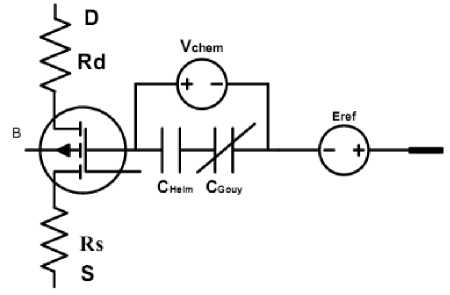
Fig. 1: Sub circuit block of ISFET macro model.
At the interface between gate insulator and the solution, there is an electric potential difference that depends on the concentration of H+ of the solution, or so called, pH value. The variation of this potential caused by the pH variation will lead to modulation of the drain current [8]. As a result, the Id-Vgs transfer characteristic of the ISFET, working in triode region, can be observed similar with that of MOSFET:
I ds = [(V gs -V th_isfet ) Vds - (V ds ) 2 ] (1)
The threshold voltage is only different in case of MOSFET. In ISFET, defining the metal connection of the reference electrode as a remote gate, the threshold voltage is given by:
Vth (ISFET) = ERef + ∆ф1j –Ψeol + χsol + ^ – Qox+Qss Q ^ox
+ γ{2φ£}1/2+ 2ф£ (2)
Where E Ref is Potential of reference electrode, ∆ф 1j is the potential drop between the reference electrode and the solution, which typically has a value of 3mV [9].
Ψ eol is the potential which is pH-independent; it can be viewed as a common-mode input signal for an ISFET interface circuit in any pH buffer solution and can be nullified during system calibration and measurement procedures with a typical value of 50 mV [10]. χ sol is the surface dipole potential of the solvent being independent of pH., the terms in the parentheses are almost the same as that of the MOSFET threshold voltage except that of absence of the gate metal function. The other terms in above equation are a group of chemical potential, among which the only chemical input parameter shown has to be a function of solution pH value. This chemical dependent characteristic has already been explained by the Hal and Eijkel’s theory [11] which is elaborated using the general accepted sitebinding model and the Gouy-Chapman-Stern model.
Why readout Circuits?
The main reason of employing a readout circuit to an ISFET circuitry, is the fact that the fluctuation of pH influences the threshold voltage, which is internal parameter of the FET and can manifest itself as a voltage signal at output but as a function of the trans conductance .The trans conductance is a passive parameter and in order to derive voltage or current signal from its fluctuations the sensor has to be attached to conditioning and transmitting circuit. In these novel designs the various current mode devices along with few passive components are used to build various readout circuits.
-
III. Current Mode Devices
-
3.1 Current Conveyor
-
3.2 DVCC
-
3.3 CDBA
In this real world most of the existing signals are analog in nature. The analog signals are act as a bridge between real world and the digital system. Initially, in the beginning of electronics Voltage mode devices are used but these devices are limited by bandwidth, slew rate, etc. Hence CMD are used because of their high bandwidth and high dynamic range. Some CMD devices are discussed briefly in the following sections
The current conveyor is a grounded three-port network represented by the black box as shown in Table 1 with the three ports denoted by x, y, and z. Its terminal characteristics can be represented best by a hybrid matrix giving the outputs of the three ports in terms of their corresponding inputs. The general Current Conveyor (CC) can be represented by the following input-output matrix relation: When a=1, the first generation current conveyor (commonly denoted CCI) is obtained [12]. For a=0, we obtain the second generation current conveyor (commonly denoted CCII). For a=-1 we obtain the third generation current conveyor (commonly denoted CCIII). Usually, b=±1. The sign of the b parameter determines the conveyor current transfer polarity. Positive b indicates that the CC has a positive current transfer ratio and is denoted by CCI+, CCII+ or CCIII+ while negative b means that it has a negative current transfer ratio and is denoted by CCI-, CCII-or CCIII-.
The differential voltage current conveyor (DVCC) is an extension of the second-generation current conveyor (CCII) introduced by Sedra and Smith [13]. Recently, the CCII has been realized using MOS transistors, with the intention to integrate the different CCII circuit applications on one chip. The CCII proves to be a versatile building block that can be used to implement a variety of high-performance circuits which are simple to construct. The DVCC is a five - port building block as shown in table. 1. It has two voltage input terminals: Y1 and Y2, which have high input impedance. The terminal X is a low impedance current input terminal. There are two high impedance current output terminals: Z1 and Z2. The DVCC is a versatile building block for applications demanding floating inputs. The CMOS realizations of this block are given. The proposed circuits are insensitive to the threshold voltage variation caused by the body effect. This minimizes the layout area and makes the circuit compatible with standard CMOS processes. The output currents (IZ1 and IZ2) follows the input current through terminal X. IZ1 has the same polarity as IX, and IZ2 is in the opposite polarity as IX. The voltage of X terminal is related by the two input voltages:
V X = V Y1 -V Y2
The current differencing buffered amplifier (CDBA) is a recently reported active component especially suitable for a class of analog signal processing applications [14]. The fact that the device can operate in both current and voltage modes provides flexibility and enables a variety of circuit designs. It has been shown that the differential nature at the input of the device considerably simplifies the implementation of CDBA-based continuous-time MOSFET-C filters in contrast to their classical operational amplifier counterparts. A block diagram of the CDBA is given in Table 1, and the behavior of the component is characterized by the following equations: shows that terminals z and w of the device can be considered as the current and voltage outputs, respectively. The difference of the input currents Ip and In , is reflected to terminal z, whereas the voltage of terminal w follows the voltage of terminal z. Moreover, the difference of the input currents is conveyed to terminal w as voltage via impedance connected to terminal z. Thus, the CDBA can be considered as a Tran’s impedance amplifier.
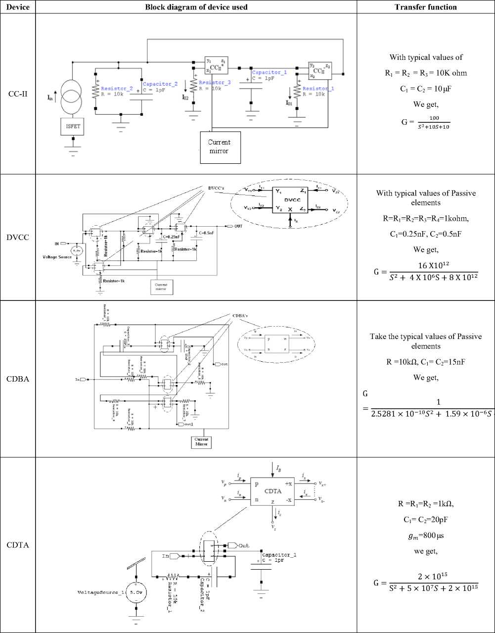
Table 1: Block diagrams and mathematical models describing the four analog CMD’s
|
Device |
Matrix Operation |
Equivalent Block Diagram |
|
CC-II |
pl Го о op-1 г, = 1 о о ?; L 0 ±1 0 vz |
X Q----- с С ------О г у о------ |
|
DVCC |
Г /yi 1 ГО 0 0 01 Г Vrl 1 1У2 _ 0 0 0 0 ^,2 Vx - 1-10 0 1х [ Iz ] [о 0 1 0 И VZ ] |
V„__ Y1 *" DVCC z Iz V,2—— Y2 lT ------Г----- V, |
|
CDBA |
V, ООО о! [7,1 ^ = 0 0 о 0 1„ I, 110 0 V, W [о 0 1 о] [zj |
VN о > N W < о Vw । CDBA l Vp a—•— P Z —«--ovz |
|
CDTA |
' I. ' 'ООО (-)П ( vz А ^ = 1 0 0 0 7„ Л £„ ООО 7, У^, ,000 0 . Jp^, |
\ о----- p +X -----о v^ ги CDTA ix : V™ ° tl z -X 1 = v,. |
Table 2: Block diagram of various devices with transfer functions
-
3.4 CDTA
Since an introduction of the current differencing trans-conductance amplifier (CDTA) in 2003, it has
been acknowledged to be a versatile current-mode active building block in designing analog circuits [15]. This device that has two current inputs and two kinds of current output provides an easy implementation of current-mode active filters. It also exhibits the ability of
Performance Analysis of Various Readout Circuits
for Monitoring Quality of Water Using Analog Integrated Circuits electronic tuning by the help of its trans-conductance gain (gm). All these advantages together with its current-mode operation nature make the CDTA a promising choice for realizing the current-mode filters. As a result, a variety of CDTA applications has also been considered by various researchers.
Inference from the table1:
-
a. CC-II
From the matrix we can deduce the following relation:
-
i y = 0;
-
v x = v y ;
-
i z = +- i x
-
• If a voltage is applied to terminal Y, an equal potential will appear on the input terminal X
-
• The current in node Y=0
-
• The current I will be conveyed to output terminal Z such that terminal Z has the characteristics of a current source, of value I, with high output impedance
-
• Potential of X being set by that of Y, is independent of the current being forced into port X
-
• Terminal Y exhibits infinite input impedance.
-
b. CDBA
The matrix shows that the difference of the input currents i p and i n is (i p - i n ) and is conveyed into the output voltage v w via external impedance connected at terminal z. The terminal z and w can be considered as the considered as the current and voltage outputs, respectively.
-
c. DVCC
While the X terminal voltage follows the voltage difference of terminals Y1 and Y2, a current injected at the X terminal is being replicated to the Z terminal. An ideal DVCC exhibits zero input resistance at terminal X, and infinite resistance at both Y terminals as well as the Z terminal.
-
d. CDTA
The matrix helps us deduce the following relations:
-
• V p = V n = 0;
-
• I z = I p – I n ;
-
• I x + = g m .V z ;
-
• I x - = -g m .V z ;
CDTA has a pair of low-impedance current inputs and p, n and an auxiliary terminal z, whose outgoing current is the difference of input currents. Here, output terminal currents are equal in magnitude, but flow in opposite directions, and the product of transconductance (g m ) and the voltage at the z terminal gives their magnitudes.
Based on the above block scheme various readout circuits involving CC-II, DVCC, CDBA, CDTA devices are designed and on the basis of the circuits transfer function of the various scheme are calculated as shown in table 2
Inference from the table2:
In this table the detailed block diagram and component description for all the four deployed techniques is given and in the adjacent column transfer functions for the corresponding block diagram has been analysed. From this table we infer the following transfer functions:
a.
CC-II - G =
100 S2+10S+10
-
b. DVCC - G =
S2+4 X 10⁶S+8 X 10¹²
c.
d.
CDBA G =------—1---------
. 5281X10 " 1 ° S2+ 1.59X10 " 6S+1
CDTA - G = ---^^---
S2 + 5 X 1 0 7 S+2 X 1 0 1 5
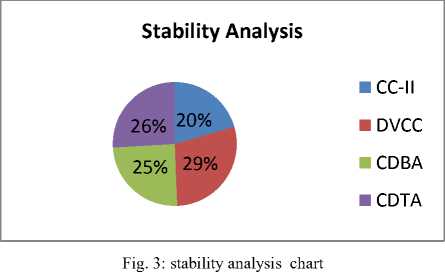
After obtaining the transfer functions for the various schemes the Nyquist and Bode plots for the various schemes are simulated on Matlab and it is found that all schemes are closed loop stable. Stability analysis that is accomplished via constructing Nyquist and Bode plots reveals that all the four techniques are closed loop stable and the phase margin (in degree) obtained from these plots follows the order listed below:
DVCC > CDTA > CDBA > CC-II
-
i .e. the phase margin is largest for DVCC followed by CDTA then CDBA and CC-II has the least phase margin.
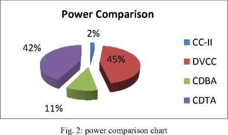
From the power comparison chart we infer that the four analog circuits used to aid the ISFET for quality measurement of water consume power in ascending order of the series given below:
CC-II < CDBA < CDTA < DVCC
Whereas from the stability analysis chart we obtain the following series:
CC-II < CDBA < CDTA < DVCC
From these two results we come down to the conclusion that although DVCC consumes more power yet it has maximum stability amongst all the other deployed circuits. Whereas if we can make a tradeoff with stability then CC-II is the best approach since it consumes least power i.e. only 2% when compared with the 45% of DVCC.
-
IV. Simulation and Results Analysis
The Circuit simulation of a water quality monitoring device using ISFET involving various CMOS analog devices is simulated on Tanner Tool version 15 for a 70 nm CMOS process model. Various parameters of interest obtained are shown in the table 4 .
Table4: Result analysis of various readout circuits
|
Parameters |
CC-II |
DVCC |
CDBA |
CDTA |
|
Technology |
CMOS |
CMOS |
CMOS |
CMOS |
|
Power supply (VDD, GND) |
5V-0V |
5V-0V |
5V-0V |
5V-0V |
|
No. of Mosfets |
16 |
100 |
64 |
32 |
|
Capacitor |
2 |
2 |
2 |
2 |
|
Current Source |
3 |
2 |
7 |
2 |
|
NMOS |
10 |
56 |
39 |
18 |
|
PMOS |
6 |
44 |
25 |
14 |
|
Resistor |
5 |
5 |
7 |
1 |
|
Voltage Source |
2 |
2 |
7 |
5 |
|
Average power dissipation (Watts) |
2.626179e-002 |
5.613851e-001 |
1.337356e-001 |
5.337467e-001 |
|
Max power (Watts) |
5.574213e-002 |
5.949921e-001 |
1.380950e-001 |
5.352302e-001 |
|
Min power (Watts) |
2.131296e-002 |
5.242404e-001 |
1.307342e-001 |
5.315526e-001 |
|
Stability analysis |
Closed loop Stable |
Closed loop Stable |
Closed loop Stable |
Closed loop Stable |
|
phase margin degree |
48.6 |
68.5 |
58.5 |
61.5 |
Inference from table 4:
For the same technology i.e. CMOS technology deployed for all the four analog IC’s and the same power supply we arrive at the following comparative results:
-
a. Number of MOSFET’s is 16 in CC-II, 100 in DVCC, 64 in CDBA and 32 in CDTA i.e. DVCC deploys maximum number of components whereas CC-II keeps it to the minimum.
-
b. Number of capacitors remains constant for all the techniques.
-
c. Number of current sources deployed is 3 for CC-II, 2 for DVCC, 7 for CDBA and 2 for CDTA i.e. in this case CDBA requires the maximum number of this component whereas DVCC and CDTA keep it to the minimum.
-
d. Number of n-MOS and p-MOS required are as follows: 10 and 6 for CC-II, 56 and 44 for DVCC, 39 and 25 for CDBA and 18 and 14 for CDTA. From these numbers we can figure out that once gain DVCC exceeds in the number of n and p type MOS whereas CC-II keep it to the least.
-
e. Number of resistors required in case of CC-II and DVCC is 5, 7 for CDBA (maximum) and 1 i.e. the least for CDTA.
-
f. Voltage source require for proper operation of the devices are 2 for DVCC and CC-II (minimum), 7 for CDBA (maximum) and 5 for CDTA.
-
g. The average power dissipation in watts is listed for the four cases:
-
1. CC-II - 2.626179e-002
-
2. DVCC - 5.613851e-001
-
3. CDBA - 1.337356e-001
-
4. CDTA - 5.337467e-001
Form this we come down to the conclusion that the average power dissipated is maximum in case of DVCC followed by CDTA; CDBA and CC-II consume the least power amongst all.
-
h. Maximum power dissipated in watts is listed for the four cases:
-
1. CC-II - 5.574213e-002
-
2. DVCC - 5.949921e-001
-
3. CDBA - 1.380950e-001
-
4. CDTA - 5.352302e-001
From this we come down to the conclusion that the maximum power dissipated is maximum for DVCC followed by CDTA then CDBA and then CC-II. As expected it follows the same precedence as in the case above.
-
i. Minimum power dissipated in watts is listed for the four cases:
-
1. CC-II - 2.131296e-002
-
2. DVCC - 5.242404e-001
-
3. CDBA - 1.307342e-001
-
4. CDTA - 5.315526e-001
From this we come down to the conclusion that the minimum power dissipated is maximum for DVCC followed by CDTA then CDBA and then CC-II. Again it follows the same pattern as the above two series which is very much expected, as well.
-
j. Stability analysis that is accomplished via constructing Nyquist and Bode plots reveals that all the four techniques are closed loop stable and the phase margin (in degree) obtained from these plots are listed as follows:
-
1. CC-II -48.6
-
2. DVCC -68.5
-
3. CDBA –58.5
-
4. CDTA –61.5
From this we understand the fact the DVCC, since its phase margin is the largest amongst all is most stable followed by CDTA then CDBA and then CC-II i.e. DVCC is most whereas CC-II is least stable amongst all.
-
V. Conclusions
In this paper, readout circuit employing second generation analog devices namely CC-II, DVCC, CDBA and CDTA is proposed. As a result of the various analysis made we arrive at the following important results:
-
a. CC-II < CDBA < CDTA < DVCC – power
consumption (in watts)
-
b. CC-II < CDBA < CDTA < DVCC – stability
The above results shows CC-II based readout circuit device consumes least power but adequate stability. On the other hand DVCC based readout circuit are more stable and consumes least power. Results of computer simulations and its comparison with experimental data and with transistor-level simulation demonstrated an accuracy of the approach. All the results are in good agreement with the theoretical analysis.
Future work
This study may be extended and more improvement in terms of power and size can be achieved at layout level and thus more effective results may be obtained.
References Performance Analysis of Various Readout Circuits for Monitoring Quality of Water Using Analog Integrated Circuits
- Ribeiro, H.M.C. Almeida, A.C. Rocha, B.R.P. Krusche, A.V. “Water Quality Monitoring in Large Reservoirs Using Remote Sensing and Neural Networks.” Latin America Transactions, IEEE (Revista IEEE America Latina) Vol: 6, Issue: 5 (2008), pp :419-423.
- Polycarpou, M.M. Uber, J.G. Zhong Wang Feng Shang Brdys, M. “Feedback control of water quality.” Control Systems Magazine, IEEE Vol: 22 ,Issue:3 (2002),pp :68-87.
- Piri, I.; Homayoonnezhad, I.; Amirian, P.; “Investigation on optimization of conventional drinking water treatment plant .” Chemical, Biological and Environmental Engineering (ICBEE), 2nd International Conference 2010 ,pp: 304 – 310.
- Hashim, U.; Haron, M.N.; “Design of digital display system for ISFET pH sensor by using PIC microcontroller Unit (MCU).” Quality Electronic Design (ASQED), 2010 2nd Asia Symposium ,Issue:1(2009), pp:148-152.
- Pawan Whig, S. N. Ahmad, (2011) On the Performance of ISFET-based Device for Water Quality Monitoring. Int'l J. of Communications, Network and System Sciences ISSN 1913-3715, pp:709 -719.
- P.Bergveld,(2000) “Thirty years of ISFETOLOGY what happened in the past 30 years and what may happen in the next 30 years,’Sens.Actuators B, Vol . 88,pp1-20.
- Sergio Martinoia and Giuseppe Massobrio (2002), A Behaviour Macro-Model of the ISFET in SPICE, Sensors and Actuators B, pp: 182-189.
- B. Palan, F.V.Santos, and J.M.Karam (1999), New ISFET Sensor Interface Circuit for Biomedical Applications, Sensors and Actuators B, pp: 63-68.
- C.H.Yang, W.Y.Chung, K.K.Lin, D.G.Pijanowska and W. Torbicz (2003), A Low-Power Telemetric System Design for ISFET-Based Sensor Array Applications, European Conf. on Circuit Theory and Design. pp: 260-263.
- Arkadiy Morgenshtein, Liby Sudakov-Boreysha and Uri Dinnar (2004), CMOS Readout Circuitry for ISFET Micro-systems, Sensors and Actuators B, (97):122-131.
- Pawan Whig, S. N. Ahmad, (2012), DVCC based Readout Circuitry for Water Quality Monitoring System, International Journal of Computer Applications (0975 – 8887) Vol. 49 pp:1-7.
- R. E. G. Van Hal, J. C. T. Eijkel and P. Bergveld (1995), A Novel Description of ISFET Sensitivity with the Buffer Capacity and Double-layer
- Capacitance as Key Parameters, Sensors and Actuators B, pp: 201-205.
- G W Roberts, A S Sedra(1989), All current-mode frequency selective circuits., Electronics Letters, 1989, 25(12),pp:759-761.
- A Sedra, K. A Smith (1970). second-generation conveyor and its applications,IEEE Transconductions on Circuit Theory. 1970, CT-17,pp: 132-134.
- W Chiu, S I Liu, H W Tsao, J J Chen(1996). CMOS differential difference current conveyors and their applications. IEEE Proceedings G: Circuits Devices Systems, 1996, 43(2),pp:91-96
- Biolek D. CDTA-building block for current-mode analog signal processing, In: Proceedings of the ECCTD’03, vol. III,Krakow, Poland, 2003. p. 397–400.
- Pawan Whig, S. N. Ahmad, (2011) Performance analysis and frequency Compensation Technique for Low Power Water Quality Monitoring Device Using ISFET Sensor. International Journal of Mobile and Adhoc Network. pp 80- 84.
