Radiation Damage Effects in Heterostructure Light Emitting Diodes (HLEDs) under Proton Irradiation Fields
 under Proton Irradiation Fields")
Author: Ahmed Nabih Zaki Rashed
Journal: International Journal of Intelligent Systems and Applications(IJISA) @ijisa
Article in issue: 5 vol.4, 2012.
Free access
In the present paper, we have been analyzed the high temperature variations testing in order to be used to determine light emitting diode lifetime, even though laser diode failure mechanisms are more sensitive to increases in current density. As a measured parameter of degradation, the current density is of great significance when searching for failure modes in a laser diode. Raising the current density however, is not really indicative of lifetime since it is more likely a situation to be avoided than one that simulates normal lifetime degradation. The reliability of semiconductor sources is very dependent on the degradation modes. This paper has investigated some of the degradation modes and capabilities of typical LEDs currently used in many communication and sensing systems over wide range of the affecting parameters. LED’s are typically used in multimode transmission systems where data rates no larger than 50 Mbit/sec are required. They have larger spectral widths and can add to the problem of dispersion in communications systems. Laser diodes are used in systems that require coherent and often single mode light such as high data rate communications and sensing applications.
Light Emitting Diodes (LEDs), Optoelectronic devices, Radiation damage, Optical functional device, Radiation efficiency
Short address: https://sciup.org/15010255
IDR: 15010255
Text of the scientific article Radiation Damage Effects in Heterostructure Light Emitting Diodes (HLEDs) under Proton Irradiation Fields
Published Online May 2012 in MECS
Photonic systems based on optical fibers, such as optical fiber sensors and data transfer systems, are ideally suited for applications where high bandwidth, immunity from electromagnetic interference, low power consumption, and low weight is recommended [1]. In order to operate such systems in a hostile radiation environment one has to know how the single components behave when they are exposed to ionizing radiation. Active devices such as light emitting diodes, laser diodes, and photo diodes are the subject of our present investigation. Light emitting diodes (LEDs) as light sources offer the advantages of simple fabrication, low cost, good linearity and small temperature dependence of the light output. Semiconductor laser diodes are emitting devices with high output power level [2], extremely narrow emission spectra and excellent mode stability (at constant temperature). A detailed understanding of proton-induced degradation in modern light-emitting diode (LED) technologies is paramount to assessing their reliability in optocoupler structures and in other applications common to many satellite designs. Our study addresses the need to develop an understanding of the types of structures and material systems that exhibit tolerance to proton degradation, and the need to gain confidence in our test methods and models for applying laboratory studies to calculate the anticipated device response in a given proton environment. We focus on LED technologies that are commonly found in commercially available devices since they are the most practical option for satellite designers. Barnes and coworkers were among the first to recognize the degradation mechanisms and relative sensitivities of GaAs based LED structures. They reported their findings in [3]. where they described the role of displacement damage in degrading the carrier lifetime and introducing defects that allow nonradiative recombination that competes with the desired radiative recombination process. In particular, they identify amphoterically doped LED structures as being especially sensitive to these effects. More recently, several groups have extended these studies to current LED technologies (some used in optocouplers) and confirmed that amphoterically doped devices appear to be much more sensitive to proton displacement effects than heterostructure based approaches.
Many improvements were made in fabrication technology for LEDs and laser diodes during the last 30 years, including the use of heterojunctions, which provide a way to adjust the bandgap by varying material composition, along with much more efficient carrier injection. The evolution of optoelectronic materials and fabrication methods is the most important factor in interpreting older data because all of the older work was done on part technologies that are so different from those in use today. In addition to the technology evolution issue, the technical points listed below are also important when interpreting older work. Comparison of Damage From Different Particle Types: Most early radiation damage studies were done with only one type of particle (electrons, protons, or neutrons), providing no direct comparison of damage between different types of radiation [4]. This, along with the developmental nature of most of the devices in earlier studies, makes it very difficult to compare older results with more contemporary work. Changes in device design and structure occurred very rapidly. It is often possible to adjust the earlier data using the more modern interpretation of displacement damage with the nonionizing energy loss (NIEL) concept [5], but caution must be used because NIEL does not necessarily address annealing or parametric dependencies for III–V technologies. Energy Dependence of Damage: Although some studies were done using particles with two or more energies, few systematic studies were done of energy dependence before 1985. The energy dependence problem was partially solved by work in the late 1980s that compared experimental results with theoretical interpretations of displacement damage [6].
Displacement damage in light-emitting diodes (LEDs) is an important issue for space applications. Some LEDs are highly susceptible to displacement damage, making them among the most sensitive components with severe degradation at very low radiation levels in environments dominated by protons. Although other types of LEDs are far less affected by displacement damage, the harder device technologies have much lower initial light output than the softer LED types. Selection of LED technologies for space is a complex issue, requiring [7] tradeoffs of several different factors. Damage in some types of LEDs is affected by injection conditions during and after irradiation [8]. This adds a further level of complexity to radiation characterization because measuring the device at high currents during a sequence of irradiation and-measurement steps will inadvertently cause some of the damage to recover, invalidating the radiation characterization for applications where the device is operated infrequently or operated at low currents. Such conditions are frequently encountered in many system applications, as well as in optocouplers (which contain LEDs). Another important factor is degradation during normal operation (wearout) which causes gradual decrease in light output [9]. Wearout degradation produces changes in LED characteristics that have many similarities to displacement damage. One question that needs to be answered is whether wearout degradation can be added independently to radiation damage, or whether it reduces or increases the sensitivity of LEDs to radiation [10].
In the present work, initial evaluations of radiation damage in these types of light emitting diodes and optical emitters were done more than 30 years ago, modern LEDs and laser diodes respond somewhat differently to radiation because of the many advances in fabrication and materials technology that have occurred during the last 30 years. It is shown that the radiation hardness for light emission in light-emitting diodes (LEDs) is substantially improved at low temperatures. The enhanced low-temperature radiation hardness for light emission in these LEDs is investigated in terms of an improvement in radiative efficiency due to a reduction of nonradiative transition probability at low temperatures. We have investigated the radiation damage effects on the LED performance characteristics such as carrier lifetime, junction current density, quantum efficiency, rise time, current gain, and transmitted signal bandwidth within LED devices over wide range of the affecting parameters.
II. LED Device Modeling Analysis
The physical mechanism which causes a degradation of the light output in irradiated LEDs is an increase of radiation-induced lattice defects [1]. Thereby non-radiative recombination centers are created which compete with radiative centers for excess carriers. This results in a decrease of the minority carrier lifetime. The ratio of the pre-irradiation (L 0 ) and post-irradiation (L) light output is given by [11]:
а "
-
| L 0 | = ^ = 1 + т 0 K ф , (1)
V L т
Where τ 0 and τ are the minority carrier lifetimes before and after exposure to a radiation dose or fluence, φ. K is a damage constant which depends on the interaction between semiconductor material and radiation field (e.g. gammas or neutrons). The exponent a varies between 1/3 and 1. The minority carrier lifetime will decrease when the product τ 0 K Ф becomes comparable with 1 and leads to a reduction in light output. Reducing the value of τ 0 K can be achieved by minimizing the pre-irradiation lifetime τ 0 . This can be accomplished by heavy doping of the emitting region and by operating the device at high current densities. Then the LED will have high pre-irradiation light output (due to a small τ 0 ) and will also be less sensitive to radiation. The ageing of the LEDs can be further accelerated by increasing the operating temperature or the current. The dependence of the mean LED life time τ on temperature and current is given by [4, 5, 12]:
-
т = CI - n exp[E^ - 1 , (2)
f I kT j J
Where I f is the forward current through the LED, T j denotes the junction temperature, and the constants C, n and the thermal activation energy E a depend on the composition and the fabrication process of the LEDs and must be determined experimentally. The diode depletion voltage, V dep >0, i.e., the voltage at which the silicon substrate is fully depleted, is proportional to the absolute value of the effective substrate doping concentration, N eff [13]:
N eff qw2 ( V deP V bi ^ ’
Where ε is the absolute silicon dielectric constant, q is the electron charge, W is the depletion region thickness, and V bi ® 0.6 Volt is the junction built-in potential. Defects generated in the diode Si substrate by neutrons cause the variation of the effective substrate doping concentration and consequently of V dep . The two microscopic mechanisms related to the N eff variation are the donor removal (in n-type silicon) and the deep acceptor level generation, which are macroscopically modeled as a function of the neutron fluence, φ by [14]:
N eff ( Ф ) = N 0 ex P (- c Ф ) - РФ , (4)
Therefore if the lifetime of the device, τ 0 is known for a given operating current, I 0 then a relationship between drive current and device lifetime can be [17]:
Solving for τ such that a relationship exists where lifetime can be predicted as a result of elevated or decreased operating drive current, I as the following expression [17]:
T = г о

Where N 0 is the donor concentration before irradiation, c is the donor removal coefficient, and β is the acceptor introduction rate. By increasing φ, N eff decreases. The diode current density at full depletion is defined by [15]:
J D A W । V = V '
The values of m range from 1.5 to 2.0, with the larger m indicating more of a reduction in operational lifetime or greater sensitivity of the device to increased currents. For determining the relationship between temperature of the device to predict lifetime an Arrhenius relationship can be expressed as:
T = Z ex P ( E a IkT ) , (12)
Where I is the diode reverse leakage current measured at V dep , A is the diode area, and W is the depletion region thickness. The J D increase is linear with fluence [16]:
J D = J 0 +г Ф
Where Г is the leakage current density increase rate and J 0 » 10 nAIcm is the diode current density before irradiation. In order to determine Г, J D has been scaled to 293 K according to [16]:
J ( T R ) = J ( T ) ( T R ) exp ^
TR " T
Where T is the absolute temperature during the I–V measurement, k is the Boltzman's constant, T R =293.16 K and the E parameter is 1.23 eV, as suggested in [16]. The lifetime of LED can be approximated by the following relationship. Given an initial power output of the device P 0 and the exponential lifetime τ, the power output over time t, can be extrapolated as:
P out ( t ) = P 0 e - t 1 T , (8)
Assume that for a given time t, the power output of the device has dropped to a percentage from the initial power level such that power ratio, P R = P out /P 0 and solve for t such that,
T = - t /ln ( P R ) , (9)
Now with t known, as well as the initial power output P 0 , the power output Pout(t) can be extrapolated over time t.
If J is defined as the current density, the lifetime of the device is defined as τ, and the empirical value parameter is defined as m, then there exists a relationship such that τ is direct proportional to J -m .
Ea is the activation energy for the device in eV, T is absolute temperature in K, and Z is the device constant in sec. The lifetime in this relationship is defined as unexceptable drive currents for lasers where the drive currents elevate to 1.2 to 1.5 times the rated drive current and for LEDs can be output power loss below that of the rated value due to point defects. For life time versus temperature calculations the following Ea, activation energies can be used [18]:
AlGaAs LEDs~ 0.5 eV, InGaAsP/InP Buried Heterostructure LED~ 0.9 eV, and GaAlAs Double Heterstructure LED~ 0.56 Ev, and Si LED~ 0.7 eV . Given a known activation energy Ea, operating temperature T 0 and lifetime of the device τ 0 , the constant Z can be calculated by the following formula:
Z = T o exp (- E a I kT o ) (1 3)
Or as a ratio, τ can be solved for in terms of T given T 0 and τ 0 such that:
T 0 _ ex P ( E a 1 kT 0 ) T ex P ( E a 1 kT )
Simplifying to solve for τ as a function of the temperature for accelerated life testing:
t = t o exp
E a
k
T 0
T
Note that for photodetectors the degradation mechanisms are different but the same Arrhenius relationship can be used to determine lifetime of the device given different operating temperatures. The same relationship holds with the activation energy being ~ 0.7 eV for infrared detectors. Also it is important to note that the criteria for detector lifetime degradation is based on receiving an unacceptable signal to noise ratio (SNR) output as a result of the accelerated temperature life test.
There has been much interest in optoelectronic integrated devices (OEIDs) [2, 5, 9]. which are important for optical information processing and optical computing. A heterojunction phototransistor (HPT) and a light-emitting diode (LED) or a laser diode (LD) are directly integrated. The HPT converts an input light to the amplified current and the LED or LD driven by current emits an intensified output light [3, 8]. The characteristics of an optoelectronic device depend on both the frequency (wavelength) and the modulation signa! frequency ofan input light. The former is called the spectral response, and the latter is the frequency response. The rise time in sec of LED can be:
T S = , (16)
g 0 n o ® p
Where G s is the signal gain, g 0 is the conversion gain of the HPT at low frequency regime, η 0 denotes the quantum efficiency for the output, and ω β is the angular frequency at current gain, β . As regards the HPT, it is often convenient to express the transistor damage as a gain damage factor, K b . Thus [19],
- - — = кь Ф(17)
PP
Current gain after a given irradiation can be calculated as the following formula:
p =---в---- ,
1 + P o K b V
A simple relation between K b and K is derived as:
Kb = — ,
® T
Where ω T is the gain bandwidth product of HPT, and ω T =β 0 ω β .
For non return to zero (NRZ) coding, the transmitted signal bandwidth based on LED device can be [20]:
B.W sig. =0.7/T S , (20)
Radiation-induced dark current density, ΔJ d can be expressed as [7, 12]:
A J d = qn i V W / K , (21)
Where q is the electron charge, n i is the intrinsic carrier concentration in cm -3 , φ is particle fluence in n/cm 2 , and W is the depletion region width in μm. Therefore the generation lifetime damage coefficient for a given particle type and energy is defined through the relation:
к = V / [( 1/ T ) - ( 1/ T o )] , (22)
The changes in LED output power related to fluence, φ, these relationships depend on the initial lifetime (τ 0 ) and the damage factor (K) can be expressed as the following formula [7, 11, 19]:
^ = ( 1 + T o к V ) ” , (23)
Where P 0 is the initial output power and P is the post-irradiation output power, and N as fitting parameter, The value of N for the single heterojunction LEDs was found to be 1.63 with a standard deviation of 0.03. The value of for the double heterojunction LEDs was 1.00 with a standard deviation of 0.04. At the very least, different devices or technologies can be compared using a Figure of Merit approach like that outlined by Ref. [21], with the suggested Figure of Merit (FOM) being :
FOM =--- P ----= ,/o , (24)
JV bias — T 0 — t o
Where P 0 is the initial output power at current density J, V bias is the bias voltage, and η 0 is the device power efficiency.
III.Simulation Results and Performance Analysis
We have investigated the performance characteristics degradation and radiation damage effects in heterostructure Light Emitting Diodes (HLEDs) over wide range of the affecting operating parameters as shown in Table 1.
Characterization of LED radiation degradation is more difficult than for conventional silicon-based electronic devices. Several factors need to be taken into account, as delineated below:
> Damage depends on current, and is generally less at high currents.
> Characteristics change as well as light output, and measurements are recommended in addition to measurement of optical intensity.
> A substantial fraction of the radiation damage may recover due to injection-enhanced annealing, which is extremely important in planning radiation tests and in interpreting test results.
> LED optical power depends on temperature, affecting measurement precision; temperature variability in the eventual application must also be considered in interpreting radiation degradation.
> Some devices may degrade in an abnormal manner, with large increases in nonradiative current at moderate injection levels.
> Degradation of light output during normal operation adds to radiation degradation and also leads to operation of devices at currents significantly lower than maximum rated values.
Table 1: Proposed operating parameters for our suggested HLED device.
|
Operating parameter |
Symbol |
Value |
|
radiation dose or fluence |
φ |
3x10¹⁴ n/cm2–5x1015 n/cm-2 |
|
Thermal activation energy |
E a |
0.4 eV–1.0 eV |
|
Acceleration factor |
C |
5–50 |
|
Junction Temperature |
T J |
285 K |
|
Device junction constant |
n |
1–2 |
|
Boltzman's constant |
k |
1.38x10⁻²³ J/K |
|
Donor concentration before irradiation |
N 0 |
1017 cm-3–1020 cm-3 |
|
Acceptor introduction rate |
β |
0.0205–0.0248 cm-1 |
|
Depletion region width |
W |
5-50 µm |
|
Donor removal coefficient |
c |
0.0008–0.002 cm-1 |
|
Absolute temperature |
T |
280 K–340 K |
|
Initial output power |
P 0 |
0.1 Watt–0.5 Watt |
|
Device time |
t |
1 msec–10 msec |
|
Operating device parameter |
α |
1/3–1 |
|
Depletion region voltage |
V dep |
1 Volt–10 Volt |
|
Optical signal wavelength |
λ |
0.65-1.3 μm |
|
Bias voltage or forward voltage |
V bias or V f |
0.5 Volt–5 Volt |
|
Initial drive current |
I 0 |
2 mA–20 mA |
|
Electron charge |
q |
1.6x10⁻¹⁹ J/ev |
|
Operating temperature=room temperature |
T 0 |
300 K |
|
Initial carrier life time |
τ 0 |
2 nsec–10 nsec |
|
Optical signal gain |
G S |
50–600 |
|
Conversion gain |
g 0 |
100 |
|
Angular frequency at current gain |
ω β |
108 Hz |
|
Quantum efficiency |
η 0 |
75%–90% |
|
Initial current gain |
β 0 |
5 |
Based on the model equations analysis, assumed set of the operating parameters, and the set of the Figs. (112), the following facts are assured as the following results:
-
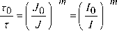
i) As shown in Fig. 1 has assured that forward voltage increases, this results in increasing of LED current. But as irradiation doses increases, this leads to decrease in LED current.
-
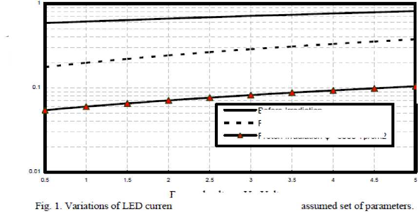
ii) As shown in Fig. 2 has demonstrated that as drive current of LED device increases, this leads to increase in LED device output power. As well as radiation doses increase, this results in decreasing of LED device output power.
-
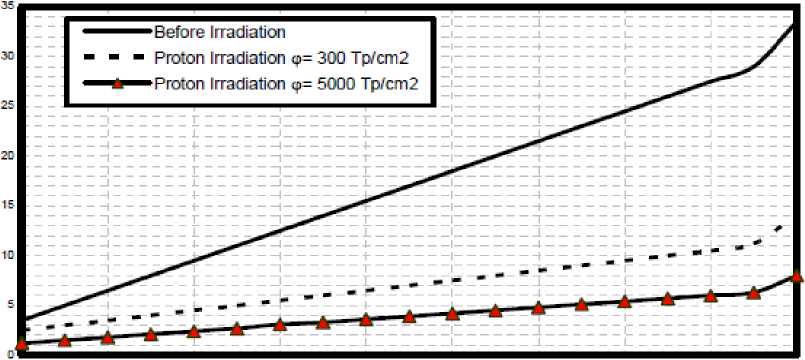
iii) Fig. (3, 4) have indicated that as both
irradiation doses and depletion region width increase, and ambient temperature decreases, this results in increasing of change of dark current.
-
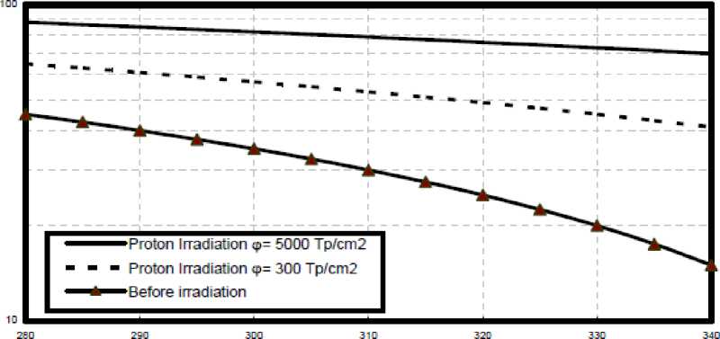
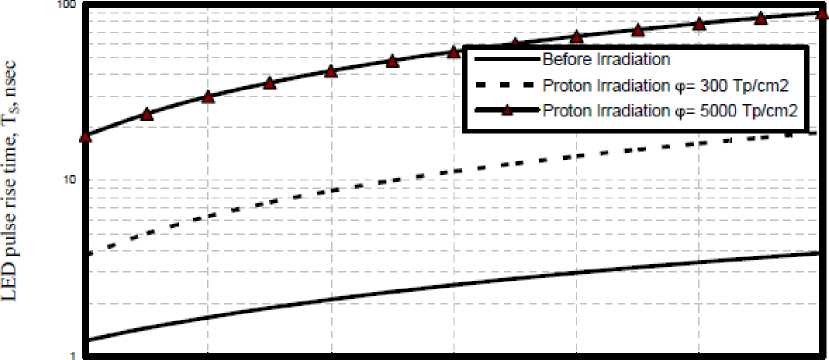
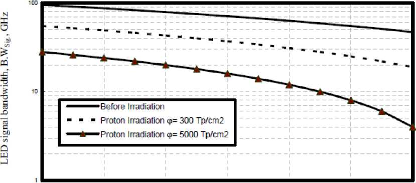
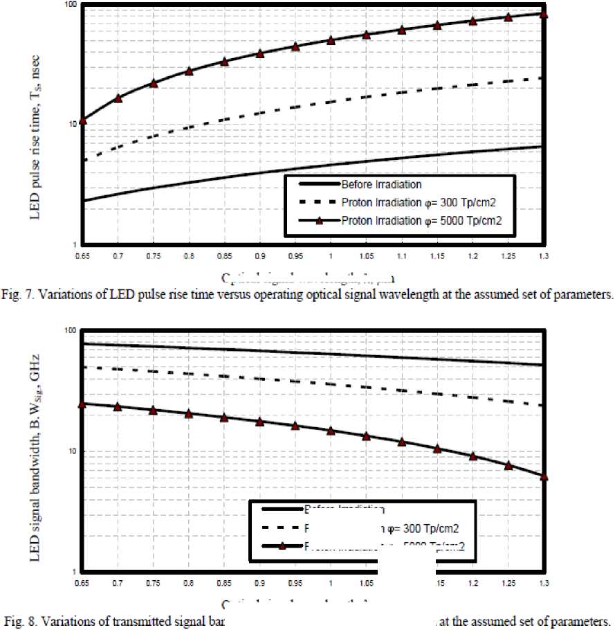
iv) As shown in the series of Fig. (5-8) have assured that as ambient temperature, operating optical signal wavelength and irradiation doses increase, this leads to increase in LED pulse rise time, and then to decrease LED signal bandwidth.
-
v) Figs. (9 , 10) have demonstrated that as bias voltage and carrier life time, and irradiation doses increase, this results in decreasing of LED device figure of merit.
-
vi) As shown in Figs. (11, 12) have indicated that as both LED output power, and quantum efficiency increases, and irradiation doses
decrease, this leads to increase in LED figure of
merit.
Forward voltage, Vp, Volt it versus forward voltage at the
Change in dark current, Altt, nA LED output power. P#, pWatt LED current, 1. mA
Before Irradiation
Proton Irradiation
Proton Irradiation ®= 5000 Tp/cm2
2 4 6 В 10 12 14 16 1B 2D
Drive current, Io, mA
Fig. 2. Variations of LED output power against drive current at the assumed set f parameters.
Ambient temperature. T. К
Fig. 3. Variations of change in dark current versus ambient temperature at the assumed set of parameters.
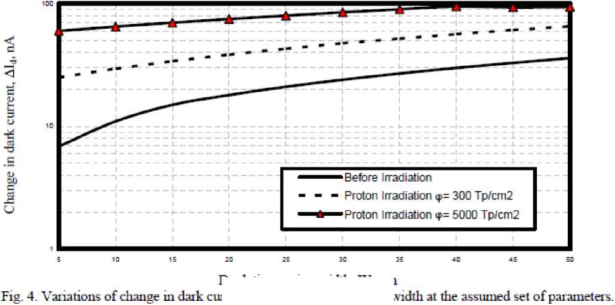
Depletion region width. W, pm inent against depletion region v
260 290 30C 310 320 330 340
Ambient temperature. T, К
Fig. 5. Variations of LED pulse rise time against ambient temperature at the assumed set of parameters.
290 290 300 310 320 330 340
Ambient temperature. T, К
Fig. 6. Variations of transmitted signal bandwidth against ambient temperature at the assumed set of parameters.
Optical signal wavelength, л, um
Before Irradiation
Proton Irradiation
Proton Irradiation
Optical signal wavelength, X, um ndwidth versus optical signal wavelength
Gamer life tune, t, nsec
Fig. 9. Variations of die figure of merit against earner life time at the assumed set of parameters.
Quantum efficiency, q
Fig 12. Variations of the figure of merit versus quantum efficiency at the assumed set of parameters.
0.75
0.78
0.81
0.84
0.87
Bias voltage, Vtias. Volt
Fig. 10. Variations of the figure of merit against bias voltage or forward voltage at the assumed set of parameters.
LED output power, Po, Watt
Fig. 11. Variations of the figure of merit against LED output power at the assumed set of parameters.
0.01
0.01
0.25
0.35
0.45
'Before Irradiation
Proton Irradiation
■Proton Irradiation
0.01
0.15
-Before Irradiation
Proton Irradiation
■Proton Irradiation
300 Tp/cm2
5000 Tp/cm2
j i
■Before Irradiation
Proton Irradiation q>= 300 Tp/cm2
Proton Irradiation q>= 5000 Tp/cm2
IV.Conclusions
In a summary, we have investigated harmful proton irradiation effects on LED devices under high thermal effects. It is theoretically found that the increased of both quantum efficiency and LED output power, and the decreased irradiation doses, this results in the increased LED figure of merit. As well as the decreased of both bias voltage and carrier life time, this leads to the increased LED figure of merit. It is evident that the decrease of ambient temperature, operating optical signal wavelength, and irradiation doses, this leads to the decreased LED pulse rise time and then lead to the increased LED signal bandwidth. Moreover the decreased ambient temperature, and the increased of both depletion region width, and irradiation doses, this results in the increased change in LED dark current. It is also indicated that the increased forward voltage and drive current, this results in the increased LED output power. But the increased of proton irradiation doses, this leads t the decreased LED output power and then to degrade LED device transmission performance.
References Radiation Damage Effects in Heterostructure Light Emitting Diodes (HLEDs) under Proton Irradiation Fields
- S. M. Khanna, D. Estan, L. S. Erhardt, A. Houdayer, C. Carlone, A. Ionascut-Nedelcescu, S. R. Messenger, R. J. Walters, G. P. Summers, J. H. Warner, and I. Jun, “Proton energy dependence of the light output in gallium nitride light emitting diodes,” IEEE Trans. Nucl. Sci., vol. 51, pp. 2729–2735, Oct. 2004.
- A. Kalavagunta, M. Neifeld, H. Barnby, and R. Schrimpf, “Impact of proton irradiation on a grating demultiplexer,” IEEE Trans. Nucl. Sci, vol. 51, pp. 3595–3602, Dec. 2004.
- J. H. Warner, R. J. Walters, S. R. Messenger, G. P. Summers, S. M. Khanna, D. Estan, L. S. Erhardt, and A. Houdayer, “High energy proton irradiation effects in GaAs devices,” IEEE Trans. Nucl. Sci., vol. 51, pp. 2887–2895, Oct. 2004.
- A. H. Johnston and T. F. Miyahira, “Energy dependence of proton damage in optical emitters,” IEEE Trans. Nucl. Sci., vol. 49, pp. 1426–1431, June 2002.
- J. Stohs et al., “Gain, refractive index change, and linewidth enhancement factor in broad-area GaAs and InGaAs quantum-well lasers,” IEEE J. Quantum Electron., vol. 37, pp. 1449–1459, Nov. 2001.
- T. F. Miyahira and A. H. Johnston, “Trends in optocoupler degradation,” IEEE Trans. Nucl. Sci., vol. 49, pp. 2868–2873, Dec. 2002.
- A. H. Johnston and B. G. Rax, “Proton damage in linear and digital optocouplers,” IEEE Trans. Nucl. Sci., vol. 47, pp. 675–681, June 2000.
- L. A. Coldren, “Monolithic tunable diode lasers,” IEEE J. Select. Topics Quantum Electron., vol. 6, pp. 988–999, Dec. 2000.
- E. Ollier, “Optical MEMS devices based on moving waveguides,” IEEE J. Select. Topics Quantum Electron., vol. 8, pp. 155–162, Jan. 2002.
- A. Johnston, “Radiation effects in light-emitting and laser diodes,” IEEE Trans. Nucl. Sci., Vol. 50, No. 3, pp.689-703, June 2003.
- K. Gill, R. Grabit, J. Troska, and F. Vasey. “Radiation hardness qualification of InGaAsP/InP 1310nm lasers for the CMS Tracker Optical Links,” IEEE Trans. Nucl. Sci., Vol. 49, No. 6, pp.2923-2929, December 2002.
- R. J.Walters, G. P. Summers, S. R. Messenger, A. Freundlich, C. Monier, and F. Newman, “Radiation hard multi-quantum well InP/InAsP solar cells for space applications,” Prog. Photovolt., vol. 8, pp. 349–352, 2000.
- P. G. Goetz, W. S. Rabinovich, R. J. Walters, S. R. Messenger, G. C. Gilbreath, R. Mohn, M. Ferraro, K. Ikossi, and D. S. Katzer, “Effects of proton irradiation on InGaAs/AlGaAs multiple quantum well modulators,” in Proc. IEEE Aerospace Conf., Big Sky, MT, Mar. 2000.
- S. M. Khanna, H. C. Liu, P. H. Wilson, L. Li, and M. Buchanon, “High energy proton and alpha radiation effects on GaAs/AlGaAs quantum well infrared photodetectors,” IEEE Trans. Nucl. Sci., vol. 43, pp. 3012–3018, Dec. 1996.
- S. M. Khanna, D. Estan, H. C. Liu, M. Gao, M. Buchanon, and A. J. Springthorpe, “1–15 MeV proton and alpha radiation effects on GaAs quantum well light emitting diodes,” IEEE Trans. Nucl. Sci., vol. 47, pp. 2508–2514, Dec. 2000.
- S. R. Messenger, R. J. Walters, E. A. Burke, G. P. Summers, and M. A. Xapsos, “NIEL and damage correlations for high energy protons in gallium arsenide devices,” IEEE Trans. Nucl. Sci., vol. 48, Dec. 2001.
- S. R. Messenger, E. A. Burke, M. A. Xapsos, G. P. Summers, R. J.Walters, I. Jun, and T. M. Jordan, “NIEL for heavy ions: An analytical approach,” IEEE Trans. Nucl. Sci., vol. 50, pp. 1919–1923, 2003.
- I. Jun, M. A. Xapsos, S. R. Messenger, E. A. Burke, R. J. Walters, G. P. Summers, and T. Jordan, “Proton nonionizing energy loss (NIEL) for device applications,” IEEE Trans. Nucl. Sci., vol. 50, pp. 1924–1928, 2003.
- Sh.M. Eladl, “Modeling of photons trapping effect on the performance of HPT-LED Optoelectronic Integrated Device (OEID),” Semiconductor Physics, Quantum Electronics & Optoelectronics Journal, Vol. 12, No. 3, pp. 255-259, 2009.
- M. V. Raghavendra, and P. L. H. Vara Prasad, “Estimation of Optical Link Length for Multi Haul Applications,” International Journal of Engineering Science and Technology, Vol. 2, No. 6, pp. 1485-1491, 2010.
- A. H. Johnston, B. G. Rax, L. E. Selva, and C. E. Barnes, “Proton degradation of light-emitting diodes,” IEEE Trans. Nucl. Sci., vol. 46, pp. 1781–1789, Dec. 1999.
