Simulation of High Step-Up DC–DC Converter for Photovoltaic Module Application using MATLAB/SIMULINK

Author: S.Daison Stallon, K.Vinoth Kumar, S.Suresh Kumar, Justin Baby
Journal: International Journal of Intelligent Systems and Applications(IJISA) @ijisa
Article in issue: 7 vol.5, 2013.
Free access
As per the present scenario lot of power shortages are there in all over the world especially country like India the grid transferring problem is also high. Almost the power from the fossil fuels are becoming so less some of the examples of the fossil fuels are (coal, lignite, oil, and gases).So most of them looking in forward for the power from green or renewable based energies like solar, wind, biomass, tidal etc. Which does not cause any pollution to the environment. In this paper the simulation and analysis of the PV panel and also high efficient boost converter design and simulation is also performed. Even though the solar based systems are renewable based energies when compared to other renewable energies like wind, biomass it does not connect to more number of grid connections. Lot of necessary steps want to be taken one of the main important factor that high efficient boost converter is needed, here in this paper the input voltage to the boost converter is given as 15V and receives the output voltage of 55.64V
AC Module, Coupled Inductor, High Step-Up Voltage Gain, Single Switch
Short address: https://sciup.org/15010446
IDR: 15010446
Text of the scientific article Simulation of High Step-Up DC–DC Converter for Photovoltaic Module Application using MATLAB/SIMULINK
Published Online June 2013 in MECS
Photovoltaic (PV) power-generation systems are becoming increasingly important and prevalent in distribution and generation systems. An conventional type of PV array is a serial connection of numerous panels to obtain higher dc-link voltage for main electricity through a dc–ac inverter. The total power generated from the PV array is sometimes decreased remarkably when only a few modules are free from shadow effects to overcome this problems several necessary steps are taken. Interactive inverter is individually mounted on PV module and operates so as to generate the maximum power from its corresponding PV module.[1]
The power capacity range of a single PV panel is about 100W to 300W, and the maximum power point (MPP) voltage range is from 15V to 40V, which will be the input voltage of the ac module; in cases with lower input voltage, it is difficult for the ac module to reach high efficiency. However, employing a high step-up dc– dc converter in the front of the inverter improves power-conversion efficiency and provides a stable dc link to the inverter. The micro inverter includes dc–dc boost converter, dc–ac inverter with control circuit as shown in Fig. 1. The dc–dc converter requires large step-up conversion from the panel’s low voltage to the voltage level of the application. The dc-input converter must boost the 48 V of the dc bus voltage to about 380– 400 V. Generally speaking, the high step-up dc–dc converters for these applications have the following common features:
-
1) High step-up voltage gain. Generally, about a step-up gain is required.
-
2) High efficiency.
-
3) No isolation is required.[2]
There are two major factors related to the efficiency of a high step-up dc–dc converter: large input current and high output voltage. Fig. 1 shows the solar energy through the PV panel and micro inverter to the output terminal when the switches are OFF.[3] When installation of the ac module is taking place, this potential difference could pose hazards to both the worker and the facilities. A floating active switch is designed to isolate the dc current from the PV panel, for when the ac module is off-grid as well as in the non operating condition.
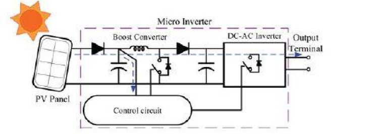
Fig .1: Block diagram of the whole system
This isolation ensures the operation of the internal components without any residential energy being transferred to the output or input terminals, which could be unsafe.
-
II. Applications of Dc-Dc High Step Up Converter
-
2.1 DC-DC Converters
2.2 Proposed Converter to Attain High Efficiency
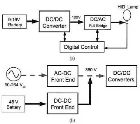
Fig. 2: shows the applications of the Boost converters, a) High intensity lamp ballast b)dual-input front –end converters
As an example for a high intensity discharge (HID) lamp ballast used in automotive head lamps in which the start-up voltage is up to 400V,an another example diagram shows the the convergence of computer and telecommunications industries in that the dc-input converter must boost the 48V of the dc bus voltage to about 380-400V. [4] The main aim here is to attain the maximum output as much we can get from the dc input similarly in this paper from the pv panel we can the dc voltage as output before connecting the output to grid the voltage from the pv panel is not more sufficient since in between the pv panels and the grid interface we are going for micro inverter which consists of boost converter and inverter. The simulation result in this paper uses 15V input to the boost converter and attains 55.64V as the output voltage respectively.[5]
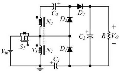
Fig .3: Proposed Converter
The proposed converter, shown in Fig.3, is comprised of a coupled inductor T 1 with the floating active switch S 1 . The primary winding N 1 of a coupled inductor T 1 is similar to the input inductor of the conventional boost converter, and capacitor C 1 and diode D 1 receive leakage inductor energy from N 1 . The secondary winding N 2 of coupled inductor T 1 is connected with another pair of capacitors C 2 and diode D 2 , which are in series with N 1 in order to further enlarge the boost voltage. The rectifier diode D 3 connects to its output capacitor C 3 .
The proposed converter has several features:
-
1) The connection of the two pairs of inductors, capacitor, and diode gives a large step-up voltageconversion ratio;
-
2) The leakage-inductor energy of the coupled inductor can be recycled, thus increasing the efficiency and restraining the voltage stress across the active switch; and 3) the floating active switch efficiently isolates the PV panel energy during non operating conditions, which enhances safety. Before get into the connection procedure we should know about the characteristics and functions of the pv panels then only it is very easy to get the maximum power output from the PV panels. [6]
-
2.3 Demands Defined by the PV Modules
Figure 4(a) model and characteristics of PV panel Electrical model with current and voltages (b) Electrical characteristic of the PV cell, exposed to a given amount of (sun) light at a given temperature. As indicated, ripple at the Photovoltaic module’s terminals results in a somewhat gives lower power generation, compared with the case where no ripple is present at the terminals. A model of a PV cell is sketched in Fig. 4(a), and its electrical characteristic is illustrated in Fig. 4(b).[3] The most common PV technologies nowadays are the mono crystalline and the multi crystalline-silicon modules, which are based on conventional, and high cost, microelectronic manufacturing processes . The MPP voltage range for these PV modules is normally defined in the range from 23 to 38 V at a power generation of more or less 160 W, and their open-circuit voltage is less than 45 V. [7] However, new technologies like thin-layer silicon, amorphous-silicon, and Photo Electro Chemical are in development. These types of PV modules can be made arbitrarily large by an inexpensive “roll-on–roll-off” process. This means that new modules with only one cell may see the light in the future. The voltage range for these cells/modules is located around 0.5 1.0 V at several hundred amperes per square meter cell. The inverters must guarantee that the PV module(s) is operated at the Maximum power point tracking, which is the operating condition where the most energy is acquired. This is accomplished with an Maximum power point tracker (MPPT). It also involves the ripple at the terminals of the PV module(s) being sufficiently small, in order to operate around the MPP without too much fluctuation.[8]
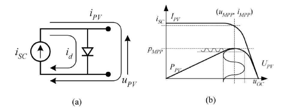
Fig. 4: Model and Characteristics of PV Panel
-
III. Simulation Results
-
3.1 Simulation of Boost Converter
-
The simulation results are shown in the figure.5, the simulation diagram and the simulation output results separately shown for the boost converter as well as inverter .The parameter values is shown below
Vs=15 V, L=1e-3H, C 1 = C 2= 47e-6 F, C 3 = 220e-6 F
R load = 400 ohms, V o =56 V
Figure 5 shows the simulation of Boost Converter using Matlab Simulink, it consists of the DC voltage source input, MOSFET switch.2 inductors,3 diodes,3 capacitors and r load the voltage measurement connected with scope to verify the simulation output results and with the signal generator to give the pulses for the circuit and finally the power GUI is connected. The main concern of this project is to design and construct a DC to DC converter which is one of the main module in the solar PV system that shown in Figure. The main principle of the DC to DC converter is based on boost type. The purpose of the project is to develop DC to DC converter (boost type) that converts the unregulated DC input to a controlled DC output with desired voltage level. The main objectives of this project are designing and constructing a DC to DC converter (boost type) circuit practically with input voltage, 15 V and the output voltage, 56 V. The output voltage waveform is mention in figure.6. [9]
Photovoltaic Module Application using MATLAB/SIMULINK
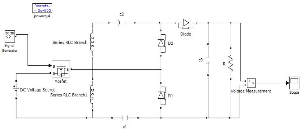
Fig. 5: Simulation of Boost Converter using Matlab/Simulink
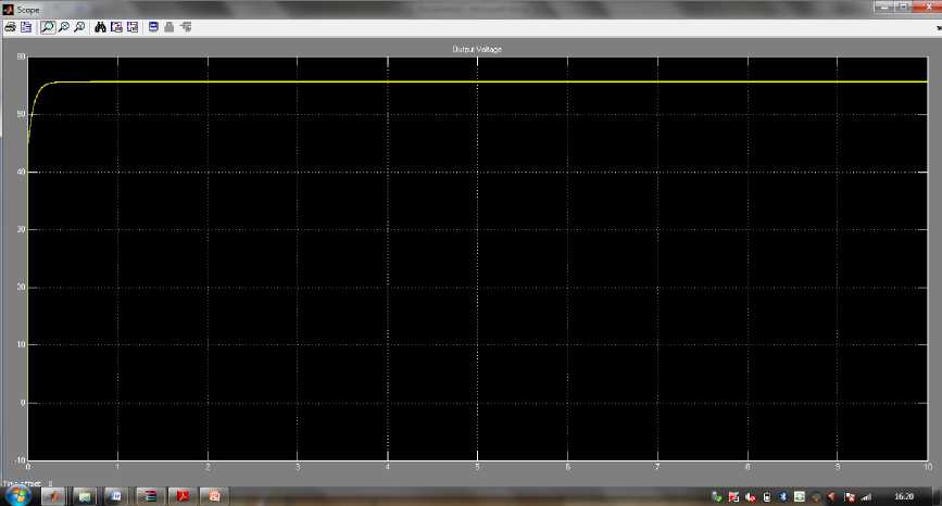
Fig .6: Output Voltage waveform of Boost Converter
-
3.2 Simulation of Single Phase Full Brige Inverter
The parameter values is shown below
V dc = 56 V
Pulse generator:
Amplitude = 1 V
Period (secs) = 0.02 sec
Pulse width(% of period) = 50%
Phase delay(secs)=0
Load:
R load =1 ohms
L load = 10e-3 H
Photovoltaic Module Application using MATLAB/SIMULINK
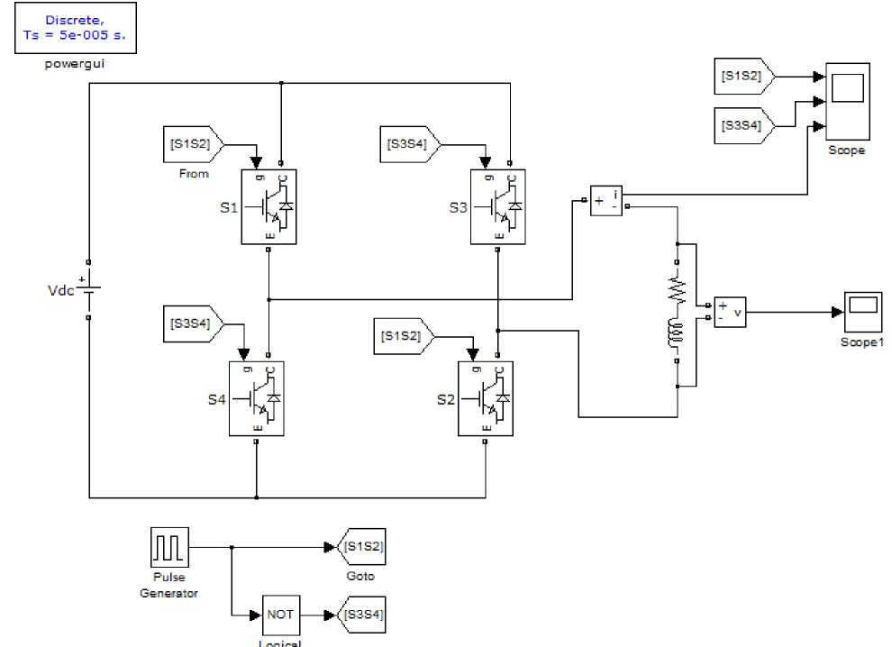
Fig. 7: Simulation of Single Phase Full Bridge Inverter using Matlab/Simulink
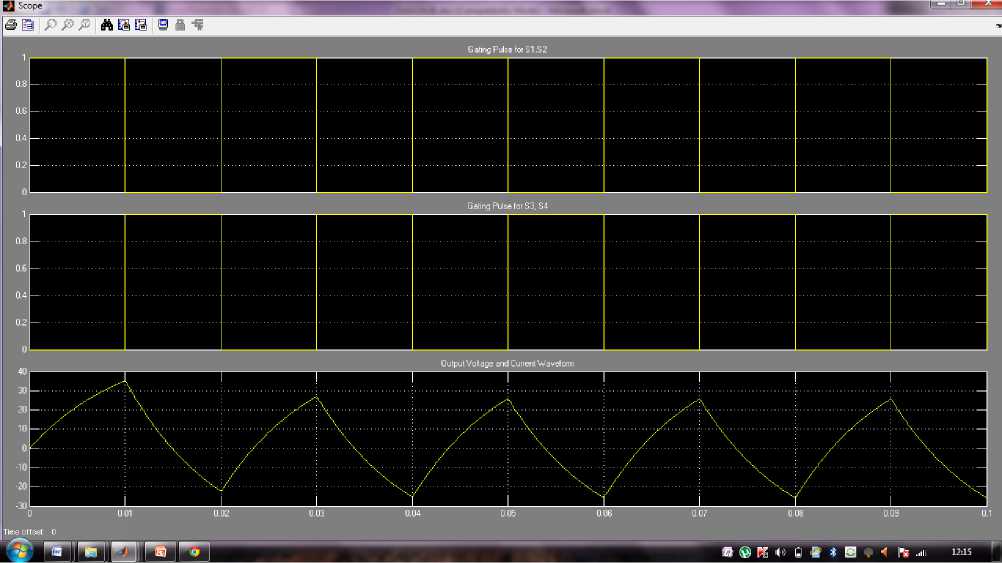
Fig. 8: Pulse voltage and Output Current waveform for Single Phase Full Bridge Inverter
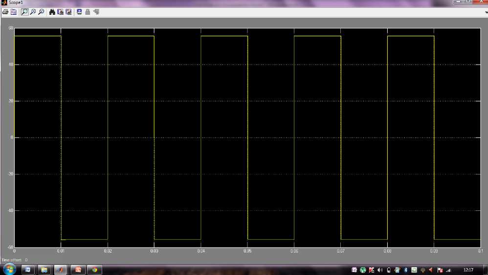
Fig. 9: Output Voltage waveform for Single Phase Full Bridge Inverter
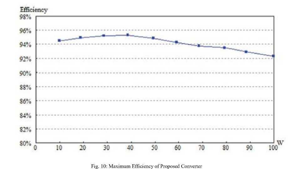
Figure. 10 shows that the maximum efficiency of 95.3% occurred at 40% of full load; and the full-load efficiency is maintained at 92.3%. The efficiency variation is about 3%, and the flat efficiency curve is able to yield higher energy from the PV module during periods when sunlight is fading. The residential voltage discharge time of the proposed converter is 480 milliseconds, which prevents any potential electrical injuries to humans.[11-12].
-
IV. Modeling and Simulation
-
4.1 Simulation of the PV panel using Matlab/Simulink
-
MATLAB/SIMULINK.
Insolation
From
Rs
-
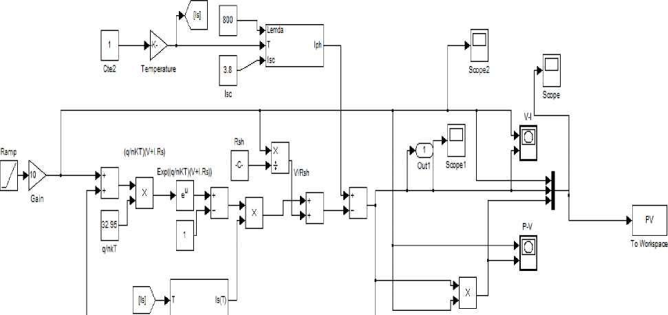
Fig. 11: Simulation of PV panel
/ q^ + ^J) Д (У+Я,1) '-'^-ц^ NKT -
- ......(1)
Where ;
I = Current to the load
Iph= Photo current
I s = Reverse saturation current of the diode q = Electron charge
V= Voltage across the diode
K= Boltzmann constant
T= Junction temperature
N=Ideality factor of the diode
Rs =Series resistors
Rsh = Shunt resistor
Based on the above equation(1) only the figure 11 is been designed .Inside this two sub systems are present . This total circuit is designed based upon the photo current, reverse saturation current of the diode, electron charge, voltage across the diode , Boltzmann constant , junction temperature , ideality factor of the diode , and finally the two important parameters are the series resistors and the shunt resistors of the cell, respectively.
The physical and also the working of the PV cell will be always in the relation with the photo current, reverse saturation current of the diode, and also the series and shunt resistors apart from this even the environmental parameters such as temperature and the solar radiation from the other side. Only by designing all the parameters we can finally attain the total PV cell. Taking into the considerations the environmental factors to be considered more important since they are also in the part to design the PV cell as well.
-
4.2 Matlab/Simulink subsystem for varying cell temperature and solar radiation
^-^ + 1.(7 - 298)]^.............(2)
Where as;
K i = temperature coefficient and the short circuit current of the cell
β = Solar radiation
Based upon the above equation (2) this subsystem has been designed. It is to be known that the PV cell current is purely dependent on the solar radiation.
Photovoltaic Module Application using MATLAB/SIMULINK
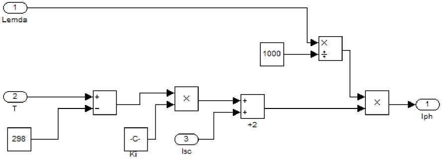
Iph=[Isc-Ki(T-298)]lemdal000
Isc^short circuit current at 25*C
Ki= cell s short-circuit current temperature coefficient in A'*c lemda: insolation in Kw/m*2
-
Fig. 12: Subsystem for varying the cell temperature and solar radiation
4.3 Matlab/Simulink subsystem for temperature effect on diode reverse saturation current
4СП - 4
Where as;
T3
nom3
exp
Lrnom Ш
I s =Diode reverse saturation current
V t =Thermal voltage
From the above equation(3) only the figure 13. is designed. In this subsystem the diode reverse saturation current and the nominal temperature, band gap energy of the semiconductor and the thermal voltage is been designed.
4.4 I-V characteristics of PV panel
T nom = Nominal temperature
E= Semi conductor band gap energy
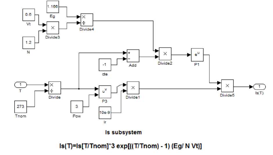
Fig. 13: subsystem for temperature effect on diode reverses saturation current
The above figure .14 shows the I-V characteristics of PV panel the X-axis is refered to the voltage (V), the Y-axis is refered to the current (I).
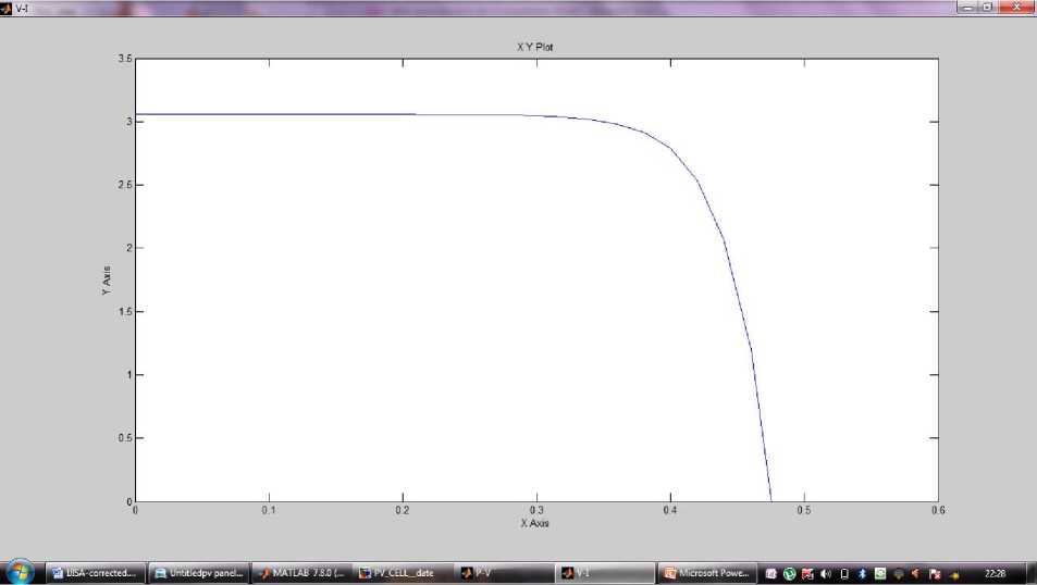
Fig. 14: I-V characteristics of PV panel
4.5 P-V characteristics of PV panel
The above figure 15 shows the P-V characteristics of the PV panel the X-axis is refered to the voltage (V),the Y-axis is refered to the power(P).
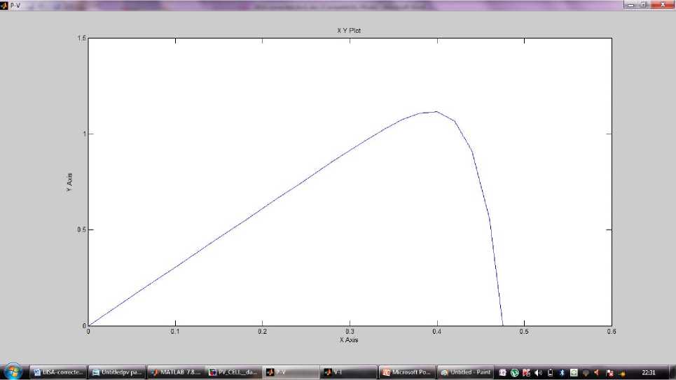
Fig. 15: P-V characteristics of the PV Panel
-
4.6 Effect of varying rs
-
4.7 Effect of varying rsh
The series resistance of the PV cell is low, and in some cases, it can be neglected. However, to render the model suitable for any given Photovoltaic cell, it is possible to vary this resistance and predict the influence of its variation on the PV cell outputs.
The shunt resistance of any PV cell should be large enough for higher output power and fill factor. In fact, for a low shunt resistor, the Photovoltaic cell current collapses more steeply which means higher power loss and lower fill factor.
-
V. Conclusion
The conventional energy resources are not enough to fulfill the needs of society, that’s the reason for going alternative energy sources like renewable energy sources. Renewable energy is the energy generated from natural resources like solar, wind and tidal etc. Solar energy is the radiant light and heat from the sun, which can be converted directly into electrical energy by using photovoltaic effect. As the temperature and isolation changes the output power will change. So in order to achieve more output power from the panel lot of measures should taken, have to reduce the shadow effect etc. Similarly from the solar PV panel lot of applications is possible, used in domestic and residential purposes, industrial sectors government buildings a huge MW rating production in the farms etc. Not only the pv panel alone can be used to give power to the grid lot of power electronics equipments are also been used to give supply to the grid the main two common power electronics equipments used in this project are dc-dc boost converter in order to obtain the maximum output voltage. To give supply to the grid we need ac supply so for that here we using inverter to convert the dc supply into ac supply. Since we have a lot of power shortages at the present scenario the alternative sources of energy especially the power that is produced from the PV panels is used all over the world. There is no doubt in future these renewable energy sources will be so useful to the human beings for their needs.
modules,” IEEE Transactions on. Industrial Electronics, 2008, 55(7): 2593–2601.
-
[3] S. B. Kjaer, J. K. Pedersen, and F. Blaabjerg, “A review of single-phase grid-connected inverters for photovoltaic modules,” IEEE Transactions on Industrial. Applications., 2005, 41(5) :1292–1306.
-
[4] B. Axelrod, Y. Berkovich, and A. Ioinovici, “Switched-capacitor/ switched-inductor structures for getting transformerless hybrid dc–dc PWM converters,” IEEE Transactions on Circuits Systems. 2008, 55(2) : 687–696.
-
[5] H. Chung and Y. K. Mok, “Development of a switched-capacitor dc–dc boost converter with continuous input current waveform,” IEEE Transactions on. Circuits Syste 1999, 46(6), : 756– 759.
-
[6] T. J. Liang and K. C. Tseng, “Analysis of integrated boost-flyback step-up converter,” IEE Proceedings of Electrical Power Applications., 2005, 152(2) : 217–225.
-
[7] Q. Zhao and F. C. Lee, “High-efficiency, high step-up dc–dc converters,” IEEE Transactions on Power Electronics, 2003, 18(1) : 65–73.
-
[8] M. Zhu and F. L. Luo, “Voltage-lift-type cuk converters: Topology and analysis,” IET Power Electronics., 2009, 2(2): 178–191.
-
[9] R. J.Wai, C. Y. Lin, R. Y. Duan, and Y. R. Chang, “High-efficiency dc–dc converter with high voltage gain and reduced switch stress,” IEEE Transactions on. Industrial. Electronics., 2007, 54(1) : 354–364.
-
[10] S. M. Chen, T. J. Liang, L. S. Yang, and J. F. Chen, “A cascaded high step-up dc–dc converter with single switch formicrosource applications,” IEEE Transactions on Power Electronics., 2011, 26(4) :1146–1153.
-
[11] L. S. Yang and T. J. Liang, “Analysis and implementation of a novel bidirectional dc–dc converter,” IEEE Transactions on. Industrial Electronics., 2012, 59(1):422–434.
-
[12] W. Li and X. He, “Review of non-isolated high-step-up dc/dc converters in photovoltaic grid-connected applications,” IEEE Transactions on. Industrial. Electronics., 2011, 58(4) : 1239–1250.
References Simulation of High Step-Up DC–DC Converter for Photovoltaic Module Application using MATLAB/SIMULINK
- T. Shimizu,K.Wada, andN.Nakamura, "Flyback-type single phase utility interactive inverter with power pulsation decoupling on the dc input for an ac photovoltaic module system," IEEE Transactions on Power Electronics., 2006, 21(5) :1264–1272.
- C. Rodriguez and G. A. J. Amaratunga, "Long-lifetime power inverter for photovoltaic ac modules," IEEE Transactions on. Industrial Electronics, 2008, 55(7): 2593–2601.
- S. B. Kjaer, J. K. Pedersen, and F. Blaabjerg, "A review of single-phase grid-connected inverters for photovoltaic modules," IEEE Transactions on Industrial. Applications., 2005, 41(5) :1292–1306.
- B. Axelrod, Y. Berkovich, and A. Ioinovici, "Switched-capacitor/ switched-inductor structures for getting transformerless hybrid dc–dc PWM converters," IEEE Transactions on Circuits Systems. 2008, 55(2) : 687–696.
- H. Chung and Y. K. Mok, “Development of a switched-capacitor dc–dc boost converter with continuous input current waveform,” IEEE Transactions on. Circuits Syste 1999, 46(6), : 756–759.
- T. J. Liang and K. C. Tseng, “Analysis of integrated boost-flyback step-up converter,” IEE Proceedings of Electrical Power Applications., 2005, 152(2) : 217–225.
- Q. Zhao and F. C. Lee, “High-efficiency, high step-up dc–dc converters,” IEEE Transactions on Power Electronics, 2003, 18(1) : 65–73.
- M. Zhu and F. L. Luo, “Voltage-lift-type cuk converters: Topology and analysis,” IET Power Electronics., 2009, 2(2): 178–191.
- R. J.Wai, C. Y. Lin, R. Y. Duan, and Y. R. Chang, “High-efficiency dc–dc converter with high voltage gain and reduced switch stress,” IEEE Transactions on. Industrial. Electronics., 2007, 54(1) : 354–364.
- S. M. Chen, T. J. Liang, L. S. Yang, and J. F. Chen, “A cascaded high step-up dc–dc converter with single switch formicrosource applications,” IEEE Transactions on Power Electronics., 2011, 26(4) :1146–1153.
- L. S. Yang and T. J. Liang, “Analysis and implementation of a novel bidirectional dc–dc converter,” IEEE Transactions on. Industrial Electronics., 2012, 59(1):422–434.
- W. Li and X. He, “Review of non-isolated high-step-up dc/dc converters in photovoltaic grid-connected applications,” IEEE Transactions on. Industrial. Electronics., 2011, 58(4) : 1239–1250.
