The influence of tunnel effect on the current injection of spin light-emitting diodes with InGaAs/GaAs quantum wells

Author: Saeid S.
Journal: Физика волновых процессов и радиотехнические системы @journal-pwp
Article in issue: 2 т.18, 2015.
Free access
By using current-voltage characteristic and electro-photo luminescence measurements, the efficiency of spin electronic injection was investigated in the Co/Al 2O 3 tunnel barrier/GaAs based structure, where spin current was generated by electric injection from FM to GaAs through the tunnel barrier. The investigations were performed on the devices with different tunnel barrier thickness of Al 2O 3 surmounted by a thin Co ferromagnetic layer. The increase of the effectiveness of the electrical injection was identified by an increase in the intensity of electroluminescence; thereby we can define the optimal thickness of the layer of Al 2O 3 as a tunnel and as a diffusion barrier. Also, manipulation of the tunneling barrier thickness leads to control of emission threshold of diode structures and sensitive diode. We also demonstrated the dependence between the tunneling barrier thickness and Schottky barrier height and the resistance of diode structure.
Spin polarization, spin injector, tunnel-thin barrier, spin-polarized charge carriers, diffusion penetration
Short address: https://sciup.org/140255918
IDR: 140255918
Text of the scientific article The influence of tunnel effect on the current injection of spin light-emitting diodes with InGaAs/GaAs quantum wells
Spintronics, in which spin degree of freedom of electrons utilize for novel electronic devices with potentially lower power consumption, faster operation and smaller size [1–2] such as spin light emitting diode (spin-LED) devices [3–4], has gained a lot of attention in recent Several decades in solid state and semiconductor Systems [5]. Spintronics, represents one of the most promising candidates as an alternative solution to standard electronics technology, which it is known will reach physical limitations in the near future [6]. Spin-LED structures have been extensively studied for development of semiconductor-based spintronics technology, because of the ease and low cost of manufacturing as well as lack of need for complex and advanced equipment for the preparation of such structures. Development of spintronic devices needs to achieve efficiently injecting spin polarized carriers from FM into a semiconductor, transporting them over reasonable distances without spin-fli pping and then efficient detection of them. Generation of spin polarization can achieve by optical techniques or by magnetic semiconductors or ferromagnetic contacts [7; 8]. In process efficient injection spin polarized carriers from FM into a semiconductor, it is created some of problems as the conductivity mismatch [9]
on interface between FM and semiconductor, it overcome this problem bye use typically a thin tunneling barrier [10–11] between FM and semiconductor as Al2O3 barrier [12–13], through MgO [13–14] and through GaO [15].
Our study was carried on the diode structures based on InGaAs/GaAs QW with FM (Co)/ Al2O3, where Al2O3 played a role of the tunnel barrier. The deposition of Co layer directly on the semiconductor leads to the emergence of several problems including: 1. Emergence of defects on the interface, which leads to an increase of relaxation speed (the speed of loss of polarization increases). 2. Diffusion of defects (impurities) into the cover layer leads to increase of dispersion as well as their arriving into the diode effective region leads to formation of the non-radioactive recombin ation centers. 3. The conductivity mismatch problem between the semiconductor and the metal, which form the basis of an obstacle in the process of spin injection.
In order to overcome these problems we used a thin tunnel barrier [16; 17] between the ferromagnetic metal and the semiconductor, which is considered as a tunnel for polarized electrons transit without resistance and without any loss of energy and spin polarization of the carriers. Thickness of the tunneling barrier plays a key role in the control of the injection process © Saeid S., 2015
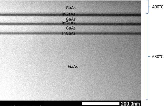
Fig. 1. Electron microscopic image of a cross section structure with three QWs
also as a diffusion barrier, which prevents the diffusion of FM cobalt atoms into the cover layer and thus reduces amount of defects in the cover layer and in the interface. Several experiments were carried to obtain the optimum value of the thickness of the tunneling barrier, which allows access to the maximum amount of spin injection.
-
1. Experimental
The studied samples were grown by metalorganic chemical vapour deposition (MOCVD) method under atmospheric pressure of hydrogen [18] for the semiconductor part and by the electronbeam evaporation method in vacuum for the tunnel barrier/ferromagnetic metal part. We have fabricated structures containing three QWs (fig. 1.) with different contents of In ( x = 0.25, 0.20 and 0.15) and located at different depths (30, 70, and 110 nm, respectively) from the surface. The QWs emit photo- or electroluminescence with different intensity and then it enabled us to measure the penetration of Co atoms into structure. We used substrates of n-GaAs (001), so that the circular polarization was due to spin-polarized holes injection from ferromagnetic contact into a semiconductor. The experiments were carried on two types of samples: 1 – samples with cover layer depositing at temperature 630 ° C, 2 — samples with cover layer depositing at temperature 400 ° C. The cover layer thickness was up to 30 nm. Also we confirmed the data obtained in the investigation of structure by transmission electron microscopy (JEM-2100F) on cross-sectional samples.
-
2. Results and discussion
The distribution of components and impurities were analyzed at the cross-sectional structure
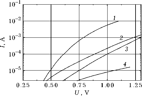
Fig. 2. The current-voltage characteristics of the diode: 1 – Al2O3 (0.5 nm)/Co/Au; 2 – Al2O3 (1 nm)/Co/Au; 3 – Al2O3 (1,2 nm)/Co/Au; 4 – Al2O3 (2 nm)/Co/Au using of Energy dispersive X-ray spectroscopy (EDS), integrated in the electron microscope. The PL was excited by He-Ne laser with power of 30 m W, and spectra PL and EL were recorded at 77 K, spectra current–voltage characteristic were recorded at 300 K and 77 K.
The fig. 2 shows, that resistance increases with tunneling barrier thickness growing and at the same 0.75 V voltage the least thickness passes the largest tunneling current. But the decrease of the tunneling barrier thickness leads to the diffusion of the larger amount of impurities into the diode structure. So there is an equation which must be achieved, that is the largest amount of electrons injected from FM to semiconductor and smallest amount of impurities diffuse into diode structure.
As a result of application of the Al2O3 film between the FM (Co) and GaAs cover layer, QW-1
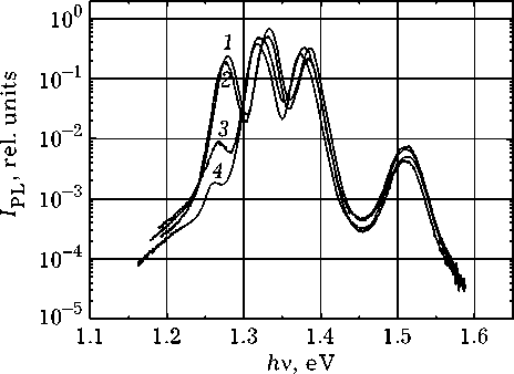
Fig. 3. The photoluminescence spectra of the structure with three quantum wells: 1 – initial sample; 2 – after deposition of Al2O3 (1,2 nm)/Со; 3 – after deposition of Al2O3 (1 nm)/Со; 4 – after deposition of Al2O3 (0,5 nm)/Со and QW-2 (fig. 3.) have not changed (intensity of PL peaks are practically unchanged). QW-3 (closest to the surface) is partially changed due to changes in the thickness of Al2O3 (intensity of PL peaks partially changed). This depends on the change of amount of Co atoms (defects) which diffuse through the tunnel-thin layer of Al2O3. Fig. 3 shows that, as a result of Al2O3 film deposition (1.2 nm) the intensity stays the same (PL intensity peaks are practically unchanged). Fig. 3 demonstrates slow penetration of Co atoms by using tunnel-thin layer of Al2O3 (≈ 1 nm thickness) as the diffusion barrier, which prevents a negative effect of luminescence quenching.
Fig. 4 shows that the Schottky barrier height of the diode structures with Au, Au /Co is relatively large and it is approximately 0.86, 0.85 eV, respectively. In forming the Co layer between the Au and GaAs, the Schottky barrier height is reduced on 0.1 eV, i.e. the height is virtually constant.
As the resistance increases slightly and its value is 0.95 Ω , the resistance is practically unchanged (fig. 5). The resistance of diode structures with Au, Au / Co is approximately 3.04, 3.994 Ω . In forming the Al2O3 tunnel barrier between Au / Co and GaAs with a thickness of 0.5 nm, the Schottky barrier height sharply decreases to 0.74 eV. This is due to the low amount of impurities diffused into the structure, and due to the tunnel effect, which allows the charge carriers to move freely between the semiconductor and the conductor.
Thus the resistance begins to increase to a value of 22.01 Ω . It should be noted that with increasing of the tunnel barrier thickness to 1 nm and then to 1.2, the Schottky barrier height increases to
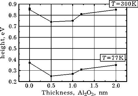
Fig. 4. Schottky barrier height dependence of the thickness of Al2O3 intermediate layer at 300 K and 77 K
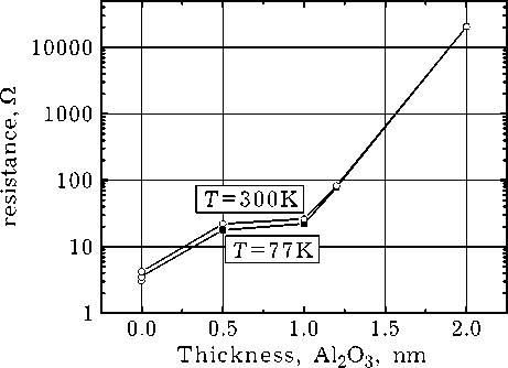
Fig. 5. The resistance dependence of the thickness of Al2O3 intermediate layer at 300 K and 77 K
0.75–0.81 eV respectively. The Schottky barrier height reaches the initial value by using a thin layer of 2 nm thickness.
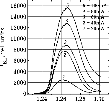
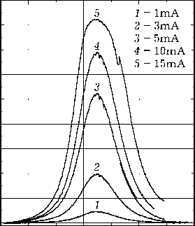
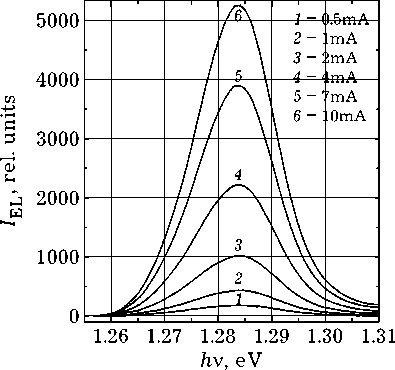
This means that the tunneling process is more difficult with increasing of the Al2O3 thickness. And it becomes almost uninteresting to us, when the thickness of Al2O3 reaches almost 2 nm. With increasing the thickness of the tunnel barrier up to 0.5, 1, 1.2 nm the efficiency of the injection gradually increased. Next, after the value of 2 nm injection efficiency decreases and becomes ineffective. It is seen that when applying electric current of 20 mA (fig. 6) the diode structure with Al2O3 thickness of 0,5nm emits electroluminescence with intensity of 2000 rel. u.
The diode structure with the Al2O3 thickness of 1 nm emits electroluminescence with intensity 5000 rel. u at the electric current of 10 mA. The diode structure with the Al2O3 thickness of 1.2 nm and the electric current of 10 mA emits electroluminescence with intensity of 14000 rel. u. This means that the electroluminescence intensity varies with the same value of the injection
-
a) hv, eV
14000 5 12000
10000 £ 8000
_ы 6000
1.32 1.34 1.36 1.38
с) hv, eV
Fig. 6. The photoluminescence spectra of the structure: 1 – after deposition of Al2O3 (0.5 nm)/Co/Au; 2 – after deposition of Al2O3 (1 nm)/Co/Au; 3 – after deposition of Al2O3 (1,2 nm)/Co/Au; 4 – after deposition of Al2O3 (2 nm)/Co/Au current by increasing the radiative recombin ation and efficient injection.
We should note that the effective injection of the charge carriers through the Al2O3 disappears at the thickness of 2 nm. This means that through such a thickness the tunneling effect disappears. Comparing the fig. 6, a and b , we see that at the current of 1 mA, the electroluminescence intensity is approximately 400, 1000 rel. u, i.e. the efficiency and sensitivity of the diode grow with the increasing of tunnel injection efficiency.
Conclusions
It has been shown that the control of the electronic injection is done by manipulation in the thickness of the tunneling barrier and thus we control intensity of radiation emitting from the spin-LED. Thus we can build a relation between the thickness insulator and the electronic injection. We showed that the optimum thickness of the tunneling barrier is between the 1–1.2 nm.
References The influence of tunnel effect on the current injection of spin light-emitting diodes with InGaAs/GaAs quantum wells
- Sarma S.D. A new class of device based on electron spin, rather than on charge, may yield the next generation of microelectronics // Am. Sci. 2001. Vol. 89. № 6. P. 516.
- Kikkawa J.M., Awschalom D.D. Lateral drag of spin coherence in gallium arsenide // Nature. 1999. Vol. 397. P. 139-141.
- Aronov A.G., Pikus G.E. Spin injection into semiconductors // Fiz. Tekh. Poluprovodn. 1976. Vol. 10. P. 1177 [Sov. Phys. Semicond. 1976. Vol. 10. P. 698].
- Comparison of Fe/Schottky and Fe/Al2O3 tunnel barrier contacts electrical spin injection into GaAs / O.M.J. van't Erve [et al.] // Appl. Phys. Lett. 2004. Vol.84. P. 4334.
- Spintronics: a spin-based electronics vision for the future / S. Wolf [et al.] // Science. 2001. Vol. 194. P. 1488.
- Zutic I., Fabian J., Das Sarma S. Spintronics: fundamentals and applications // Rev. Mod. Phys. 2004. Vol. 76. P. 323.
- Engel H.-A., Recher P., Loss D. Electron spins in quantum dots for spintronics and quantum computation // Solid State Commun. 2001. Vol. 119. P. 229; Electrical spin injection from ferromagnetic MnAs metal layers into GaAs / M. Ramsteiner [et al.] // Phys. Rev. B. 2002. Vol. 66. P. 081304.
- Injection and detection of a spin-polarized current in a light-emitting diode / R. Fiederling [et al.] // Nature. 1999. Vol. 402. P. 787-790; Spin injection into semiconductors / M. Oestreich [et al.] // Appl. Phys. Lett. 1999. Vol. 74. P. 1251.
- Fundamental obstacle for electrical spin injection from a ferromagnetic metal into a diffusive semiconductor / G. Schmidt [et al.] // Phys. Rev. B. 2000. Vol. 62. P. R4790.
- Rashba E.I. Theory of electrical spin injection: tunnel contacts as a solution of the conductivity mismatch problem // Phys. Rev. B. 2000. Vol. 62. P. R16267.
- Semiconductors between spin-polarized sources and drains / A. Fert [et al.] // IEEE Trans. Electron Devices. 2007. Vol. 54. № 5. P. 921-932.
- Electrical spin injection into -doped quantum dots through a tunnel barrier / L. Lombez [et al.] // Appl. Phys. Lett. 2007. Vol. 90. P. 081111.
- Spin-polarized electroluminescence and spin-dependent photocurrent in hybrid semiconductor/ferromagnetic heterostructures: an asymmetric problem / P. Renucci [et al.] // Phys. Rev. B. 2010. Vol. 82. P. 195317.
- High speed pulsed electrical spin injection in spin-light emitting diode / V.G. Truong [et al.] // Appl. Phys. Lett. 2009. Vol. 94. P. 141109.
- Efficient spin injection into semiconductor from an tunnel injector / H. Saito [et al.] // Appl. Phys. Lett. 2010. Vol. 96. P. 012501.
- Band offsets at and interfaces / H.B. Zhao [et al.] // Appl. Phys. Lett. 2003. Vol. 82. P. 1422.
- Optical investigation of electrical spin injection into semiconductors / V.F. Motsnyi [et al.] // Phys. Rev. B. 2003. Vol. 68. P. 245319.
- Применение лазерного распыления для получения полупроводниковых наногетероструктур / Б.Н. Звонков [и др.] // Опт. журнал. 2008. Т. 75. № 6. С. 56-61.
