Theory of absorption of gamma rays on the surface and internal of sio2 Nano powder

Author: Elchin Huseynov, Lu Jin
Journal: Science, Education and Innovations in the Context of Modern Problems @imcra
Article in issue: 1 vol.8, 2025.
Free access
We have theoretically investigated gamma rays absorption on the nanosilica surface. Calculations revealed that absorption of gamma rays was observed not only on the surface, but also inside of SiO2 nanopowder, because radiation effects of selected nano-particles more than the macro-particles. If the system gets 20000 photons; 0,0576 photons absorbs in 20nm thickness (this is same silica nanopowder diameter), 2,879796797 photons in 1μm thickness and 2682,24863 photons in1mm thickness. Nano silica has more surface, therefore, more surface effects and absorption of gamma rays on the surface has got in this sample. We also take out specific equation for absorption gamma ray on the nanosilica surface. We have investigated the effects of secondary electrons and photons emitted from surrounding materials on defect formation in silica nanopowder under γ-ray irradiation.
Nanosilica, silica nanopowder, radiation effects, nanotechnology, γ-irradiation of SiO2
Short address: https://sciup.org/16010353
IDR: 16010353 | DOI: 10.56334/sei/8.1.46
Text of the scientific article Theory of absorption of gamma rays on the surface and internal of sio2 Nano powder
“Gamma rays” is the name given to high energy electromagnetic radiation originating from nuclear energy level transitions. In this case typical wavelength, frequency, and energy ranges are: 0.0005 to 0.15 nm, 2 × 10¹⁸ to 6 × 10²⁰ Hz, and 10 keV to 2.5 MeV, respectively. The terms gamma rays, nuclear x-rays, and high-energy photons are often used interchangeably. Gamma rays traversing matter are absorbed due to a number of processes. The ability of a substance to absorb gamma rays is expressed by the absorption coefficient for that substance. In this experiment an attempt will be made to verify the theoretical expression describing the absorption of gamma rays as a function of absorber especially nanomaterial and the absorption coefficients for lead and SiO2 nanopowder and SiO2- H2O nanocomposite for gamma rays from Co-60 will be measured and compared to accepted values.
Gamma ray absorption is a random type of process; it is not possible to say whether a particular gamma ray will interact with the absorber or pass through unaffected. The processes by which gamma ray absorption occur are: 1) the photoelectric effect; 2) Compton scattering, and; 3) pair production. The photoelectric effect and Compton scattering are discussed in experiments 5 and 6 respectively. Pair production is the process whereby, in the vicinity of a nucleus, a photon (gamma ray) spontaneously materialises into an electron and a positron. Pair production can only occur for gamma ray energies ≥ 1.02 MeV. In all three of these processes the gamma ray is either scattered away from the incident direction or completely absorbed. That is, if a detector is placed on the opposite side of the absorber, along the incident direction of a beam of gamma rays, only those gamma rays which did not interact with the absorber will be detected.

Sci. Educ. Innov. Context Mod. Probl. P-ISSN: 2790-0169 E-ISSN: 2790-0177 Issue 1, Vol. 8, 2025, IMCRA of the irradiation effects it has been applied the total incident gamma quanta fluence, as well as, the so called exposition doses.
During the irradiation of high-energy photons, various surrounding materials around a specimen, i.e. a sample holders, container, etc., must emit secondary electrons and photons from their surfaces and could add some irradiation effects on the direct irradiation of the specimen. Nevertheless, the effects of the secondary electrons and photons coming from the surrounding materials have not been studied systematically. In order to demonstrate that the influence of the surrounding materials on the defect formation in the covalent bonding materials, we have irradiated SiO 2 (silica) nanopowder, which this powder synthesis of sol-gel proses [1].
However, from all point defects induced by gamma ray transport in solids, atom displacements might induce a large time scale target properties modification because of the huge time of life of induced vacancies and interstitial Frenkel pairs defect in target crystalline structure. Therefore, gamma radiation damage in solids is commonly described by the spatial dpa distribution. However, because of the insignificant photon transferred energies in their interactions with atoms, secondary electrons must be considered as the unique particles transferring enough recoil energy to the target atoms for leaving their crystalline sites leading to atom displacements processes in solids
Theatrical background. Gamma rays within the energy range produced by Co-60 source interact with nano SiO 2 powder and SiO 2 -H 2 O nanocomposite via three primary mechanisms: photoelectric absorption, Compton scattering, and pair production. In photoelectric absorption, the incident gamma ray is absorbed by the atom as a whole which results in the ejection of one of the inner shell electrons. The ejected electron's kinetic energy, T, is given by T = E γ - E b , where Eγ is the incident gamma energy and Eb is the ejected electron binding energy. The binding energy is generally insignificant in comparison with E γ . In the particular case of source, the low energy photons for which E b is a significant fraction of Eγ have such short path lengths that they do not penetrate the fuel cladding. The electron binding energy is therefore neglected in this study. No single theoretical expression accurately describes the probability for photoelectric absorption throughout the energy range of interest. This study, therefore, uses the
Sci. Educ. Innov. Context Mod. Probl. P-ISSN: 2790-0169 E-ISSN: 2790-0177
Issue 1, Vol. 8, 2025, IMCRA numerical values for the photoelectric absorption cross section (tabulated as a function of incident gamma energy) found in the X-ray information data base of the national nuclear data center. The differential probability per SiO2 molecule that an incident gamma of energy Eγ will excite an electron to energy within dT of T through photoelectric absorption is given by
S a pe ( E . , , T) S a pe ( E , , t ) dE d a pe ( E , ) ,
)
0 T = d E = 8 E y - T (1)
dT dEY where the superscript pe denotes photoelectric absorption, dEγ/dT = 1, and a pe(E, ) = a s'(E, )+ 2a /(E, ) (2)
Compton scattering is the dominant mechanism for energy loss in silica for photons with energies between roughly 60 keV and 10 MeV [2]. The vast majority of gamma rays produced by nuclear reactors lie within this energy region. In Compton scattering the incident photon scatter off an electron in the absorbing material. As the photon is deflected, it transfers some of its energy to the struck electron. The energy transfer is described by the Klein-Nishina formula. The differential cross section per electron in the absorbing material for the production of and electron of energy within dT about T by Compton scattering is given by
-----Y---=—0--e—^2 + 1 I 11^- I d T E 2 Ie- t 1 11 e 1
Y [ I Y J [I Y J
E - T 2 m c 2 ( E - T ^1] cm 2
—Щ (3)
E E । T ^ eV • electron
Y Y к Jj]

Sci. Educ. Innov. Context Mod. Probl. P-ISSN: 2790-0169 E-ISSN: 2790-0177
Issue 1, Vol. 8, 2025, IMCRA where r0 = 2,818 x 10-13 cm and mec2 = 5,11 x 10⁵ eV. Considering energy and momentum conservation laws, however, the maximum energy, Tm, that Compton scattering can transfer to the struck electron is
T
m
In the vicinity of a nucleus, gamma rays with energy greater than 1.022 MeV can undergo pair production yielding an electron-positron pair. In the process the nucleus recoils with negligible energy and the electron and positron share the remainder of the gamma energy not used in their creation [3]. The energy can be divided into any fraction between the two particles. However, since almost all gamma rays at nuclear reactors have energy less than 10 MeV and the constituent atoms of SiO2 have relatively low atomic numbers, pair production is a low probability event and thus simplifying assumptions about the energy distribution of the electron-positron pair can be made without significantly effecting the model predictions. Therefore, it is assumed that the excess photon energy is divided equally between the two particles, so that for each change in the incident gamma energy the electron changes energy by one half (dEγ/dT = 2). Also it is assumed that positrons interact with SiO2 just the same as electrons.
Gamma rays with energy above 4mec2 (2,044 MeV) can also pair produce in the vicinity of an electron. Since this is an even lower probability event than nuclear field pair production, simplifying assumptions about the energy distribution among the recoil electron and the created electron-positron pair result in only a negligible overall error [4]. This study assumes that the excess energy is divided equally among the particles (dEγ/dT = 3). As in nuclear field pair production, positrons are assumed identical to electrons. The cross sections for pair production in both nuclear and electron fields are obtained from the national nuclear data center X-ray information database. The differential cross sections for producing electrons within dT of T by an incident photon of energy EY by nuclear and electron field pair production used in this study are
do ppn (Ey ,T) do ppn (Ey ,T) dEY dо ppn (EY ) ( Ey -1,022MeV ^
Sci. Educ. Innov. Context Mod. Probl. P-ISSN: 2790-0169 E-ISSN: 2790-0177 Issue 1, Vol. 8, 2025, IMCRA do ppe (EY , t) do ppe (Ey , t) dEY dо ppe(Ey ) ^ EY - 2,044MeV ^
----—----= 3 d E y — 9 6 I - T \ (6) dT dE y ^ 3 )
where the superscript ppn and ppe denote nuclear and electron field pair production, respectively.
The factor of two in the nuclear field pair production differential cross section formula arises because both a positron (assumed identical to an electron) and an electron are produced in the reaction. Also the factor of three in the electron field pair production differential cross section formula arises because three energetic particles result from the interaction. σppn(Eγ) and σppe(Eγ) are the molecular pair production cross sections given respectively by о ppn (Ey ) —о ppn (E )+ 2o ppn (E )
, Si y
о ppe ( E
) = о ppe ( E ) + 2 o ppe ( E )
Y Si Y
Combining the differential energy transfer cross sections with the gamma flux yields the energetic electron source energy spectrum for SiO2 in a typical nuclear reactor environment, deT) E'(max) dф до (E ,T)
= J -1-----7---dEy dT 0 dEy where до (Ey , T) до c (Ey , T) до pe (Ey , T) до ppe (Ey , t) до ppn (Ey , t)
— + ++ д T д T д T д T
ϕ γ is the gamma flux and β(T) represents an electron of energy T.

Sci. Educ. Innov. Context Mod. Probl. P-ISSN: 2790-0169 E-ISSN: 2790-0177 Issue 1, Vol. 8, 2025, IMCRA
The following definitions are necessary to formulate the equations for the damage energy and the net atomic displacement: (1) s i (E) is the electronic stopping power per unit atomic density for type i particles; (2) f j is the atomic fraction of type j atoms; (3) dσi j (E, T)/dT is the differential cross section for a type i particle of energy E to transfer energy T to a type j particle; (4) ν i (E) is the damage energy which will be deposited in a material by a type i particle of energy E; (5) ρ j (T) is the probability that an initially bound atom of type j when receiving energy T in a collision will be displaced; (6) λ ij (E) is the probability that a type i atom left with energy E after displacing a type j atom will be trapped at the type j site; and (7) gi j (E) is the average number of type j atoms displaced and not recaptured in subsequent replacement collisions in a displacement cascade initiated by a type i primary knock-on atom [5].
Coulter and Parkin's representation of Lindhard et al.'s polyatomic damage energy function is given by
( ) Me)
“ijE da ,j(E,T){
) ( )( )
si E dE = f J dT V'E - T—V E+Г/ TdT
J = 1 0
Also, Parkin and Coulter's net atomic displacement function is dg (E ) m ^E da (E,T )
s ( E ) j - £ f -^ -----{ [ 1 - p ( T > ( E - T )] g ( E - T ) - g ( E ) + p ( T ) g ( T ) } dT (11)
dE k J dT , . ij
ij k kj
k = 1 0
Before the integral equations describing charged particle radiation damage in solids can be solved, the charged particle interaction parameters need to be obtained. This includes the electronic stopping power, nuclear energy transfer cross section, and the atomic displacement and capture probabilities.
Sci. Educ. Innov. Context Mod. Probl. P-ISSN: 2790-0169 E-ISSN: 2790-0177
Issue 1, Vol. 8, 2025, IMCRA
Although general notation has been used for the displacement probability, ρj(T), and the capture probability, λij(E), the detailed data about the interatomic potentials of SiO2 glass required to implement the scheme art not available. Instead simple sharp threshold forms were used in all calculations.
/ x Io for ... T < Ed
P ( ) =
k
T -I
1 for...T > Ed
^ ) I1 for ... E < Ecap
X E = - ik
ik l0 for . E > Ecap
EE where d is the average kinetic energy required to displace a type k atom, and cap is the average ik
k maximum residual energy that a type i atom, which has just displaced a type k atom, can have and be trapped in the type k site. The size of these energies can be estimated using an argument due to Seitz. Seitz's estimate for the displacement threshold is 2-2,5 times the average bonding energy. The Si-O bonds are about 4,5 eV. Since SiO2 is tetrahedrally bonded this yields estimated displacement thresholds of 20 eV for oxygen atoms and 40 eV for silicon atoms. The like atom capture energy is simply the displacement energy ( Ecap = Ed ). Since silica has about 50% ionic bonding character, the capture ii ii probability for unlike atoms is nearly zero.
Calculations. An expression can be derived which gives the number, N , of gamma rays that will pass through an absorber without interacting, as a function of the absorber nanomaterial size and the incident number of gamma rays. Consider a number, N o, of gamma rays incident on an absorber of “selected thickness” d . Suppose the absorber include n particle on “selected thickness” and per nanoparticle size diameter equal to Δd (see Figure 1).

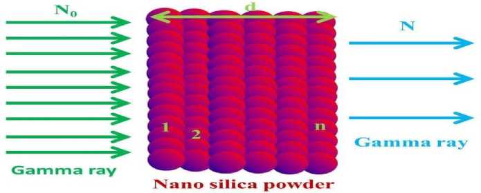
-
Figure 1.
Since gamma ray absorption is a random process, it is reasonable to expect that the change in the number of gamma rays, Δ N , due to absorption in a section of the absorber, is proportional to the number of gamma rays incident on the absorber section (per particle) and the absorber section “selected thickness”:
∆ N ∞ N ∆ d (13)
That is, the likelihood of a gamma ray interacting increases as the silica nanoparticle of the absorber “selected thickness” increases, and increasing the number of incident gamma rays increases the number that will be absorbed. To make equation (13) an equality, define μ, the absorption coefficient, as
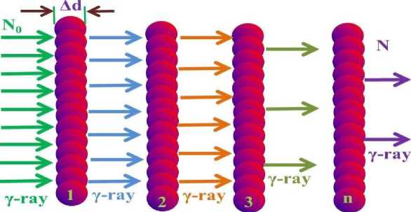
Nano silica powder
-
Figure 2
Sci. Educ. Innov. Context Mod. Probl. P-ISSN: 2790-0169 E-ISSN: 2790-0177 Issue 1, Vol. 8, 2025, IMCRA
The relative change in the number of gamma rays, due to absorption, is
A N
N
Consider the absorber to be separated SiO2 nanoparticle. The number of gamma rays remaining after each silica nanoparticle of the absorber is traversed is given by;
-
- — N = N ( 1 - A N ^ = N ( 1 - ЦА d )
N = N
-
1 0 0
N 0 1 N J 0
AN
N
A.d N = N ( 1 - ’ is the ........ „..ining .„ pa...... .rough - com,..
n 0
Now recall that Ad= d/n.
( Ц d ^ n
Nn = N о 1 1 - I (17)
Note that the above analysis assumes that the number of gamma rays changes linearly over the width of each absorber SiO2 nanoparticle. For example: for N1 we can write
N 1 = N 0 – N 0 μΔd = c 1 + c 2 Δd (c 1 and c 2 constant)
However, the proper expression is N = No - N'цАd , where N' decreases continuously as the gamma rays pass through the absorber silica nanoparticle. This problem can be overcome by taking smaller and smaller nanoparticle. Therefore, from equation (17):
N = lim N
Sci. Educ. Innov. Context Mod. Probl. P-ISSN: 2790-0169 E-ISSN: 2790-0177 Issue 1, Vol. 8, 2025, IMCRA
A N
N dN = -цд d lim implies___ ц
A d ——0 ^N
d dN
N N 0
Л f
Sci. Educ. Innov. Context Mod. Probl. P-ISSN: 2790-0169 E-ISSN: 2790-0177 Issue 1, Vol. 8, 2025, IMCRA
N In N — In N о — — ц d
N — N e~цd
That is, the number of gamma rays remaining decreases exponentially as the absorber thickness is increased. Although the desired result follows rather easily by integrating equation (15), such is not always the case. In this instance, equation (15) can be written as dN
— ц N
dd which is an easily solved differential equation. However, for some types of problems, the differential equation may be quite complicated. In that case, it is useful to use an iterative type of solution as was done initially. Also, note that the iterative calculation lends itself rather nicely to computer programming.
Finally, we can make some changes on equation (18) for explanation how the gamma rays absorbs on the SiO2 nanopowder surface same figure 1. Thus, from equation (18) we can write as follows:
-
— Ц pA d p
N — N 0 e (19)
where, p - material density (g/cm 3 ) and ц
= S - Mass Attenuation Coefficient or Specific Surface Area of nanopowder (MAC or SSA), (cm2/g).
For absorbing gamma rays in each layer of nanosilica powder as shown in the figure-2 can be written following way according to the equation (16):
Sci. Educ. Innov. Context Mod. Probl. P-ISSN: 2790-0169 E-ISSN: 2790-0177 Issue 1, Vol. 8, 2025, IMCRA
If we take an account the density of the sample 0,9g/cm3, the specific surface area 160m2/g and thesizes of nanoparticles 20nm, then we can calculate the absorption of gamma rays for each layer:
N 1 = N 0 (1-160x0.9x20x10-9) = N 0 (0.99999712)
for n layer
N 1 = N 0 (0.99999712)n
If we assume that the number of photons falling to the surface is 20000, then the absorbed gammarays in the SiO 2 nanopowder we can calculate as follows:
N absorb = N 2 – N 1 = 0.0576
The absorbed doses on the SiO2 nanopowder in the thickness of 1μm and 1mm respectively, canbe calculated as follows:
N μm = 20000-N μm (0.99999712)50 =
2.879796797 N mm = 20000-
N mm (0.99999712)50000 = 2682.24863
If the system gets 20000 photons; 0,0576 photons absorbs in 20nm thickness (this is same silica nanopowder diameter), 2.879796797 photons in 1μm thickness and 2682.24863 photons in1mm thickness. Taking into account that, the number of photons N directly related to gamma ray intensity I or dose D. Then we can lead assumptions similar calculations for intensity and radiation dose.
Radiation damages in covalent bonding materials (semiconductors and insulators) have been investigated for their useful application in fission and fusion reactors. Irradiation of energetic ions, electrons, neutrons and photons (X-rays and γ-rays) induces electron excitation and atomic displacement. In these materials, the electron excitation in radiation field plays an important role on degradation of optical and electric properties of those materials [6-7].
Results. Calculations revealed that absorption of gamma rays was observed not only on the surface, but also inside of SiO 2 nanopowder, because radiation effects of selected nano-particles more than the macro-particles. We have theoretically investigated gamma rays absorption on the nanosilica surface. If the system gets 20000 photons; 0,0576 photons absorbs in 20nm thickness
Sci. Educ. Innov. Context Mod. Probl. P-ISSN: 2790-0169 E-ISSN: 2790-0177 Issue 1, Vol. 8, 2025, IMCRA
(this is same silica nanopowder diameter), 2,879796797 photons in 1μm thickness and 2682,24863 photons in1mm thickness. Nano silica has more surface, therefore, more surface effects and absorption of gamma rays on the surface has got in this sample. We also take out specific equation for absorption gamma ray on the nanosilica surface. We have investigated the effects of secondary electrons and photons emitted from surrounding materials on defect formation in silica nanopowder under γ-ray irradiation.
