Ultra Wide Wavelength Multiplexing/Demultiplexing Conventional Arrayed Waveguide Grating (AWG) Devices for Multi Band Applications
 Devices for Multi Band Applications")
Author: Abd El–Naser A. Mohamed, Ahmed Nabih Zaki Rashed, Mahmoud M. A. Eid
Journal: International Journal of Intelligent Systems and Applications(IJISA) @ijisa
Article in issue: 2 vol.4, 2012.
Free access
This paper has proposed new materials based conventional arrayed waveguide grating (AWG) devices such as pure silica glass (SiO2), Lithium niobate (LiNbO3) , and gallium aluminum arsenide (Ga(1-x)Al(x)As) materials for multiplexing and demultiplexing applications in interval of 1.45 μm to 1.65 μm wavelength band, which including the short, conventional, long, and ultra long wavelength band. Moreover we have taken into account a comparison between these new materials within operating design parameters of conventional AWG devices such as diffraction order, length difference of adjacent waveguides, focal path length, free spectral range or region, maximum number of input/output wavelength channels, and maximum number of arrayed waveguides. As well as we have employed these materials based AWG to include Multi band applications under the effect of ambient temperature variations.
Diffraction order, Multi band wavelengths, Ultra long wavelength band, Arrayed waveguide grating (AWG), Multiplexing/Demultiplexing applications
Short address: https://sciup.org/15010096
IDR: 15010096
Text of the scientific article Ultra Wide Wavelength Multiplexing/Demultiplexing Conventional Arrayed Waveguide Grating (AWG) Devices for Multi Band Applications
Published Online March 2012 in MECS
The increase on the demand of these services, related to the deregulation processes in USA and Europe in the telecommunications sector [1], has motivated the need of telecommunication transport networks with higher capacity and flexibility. Hence, the general trend in the all the disciplines of telecommunications in the last decade, has been the increase of the capacity and flexibility of existing networks, and the deployment of new networks to cope with the mentioned demand. Therefore, new technologies have appeared and been developed in this period. The discipline of photonics and fiber optic communications has attracted a lot of interest, and has been one of the fields with major increase during this period. Several photonics and optics technologies have made feasible the increase and development of the capacity and flexibility in existing and new telecommunications networks. Nevertheless, two optic technologies have been recognized as the main contributors. First, optical amplification, which has enabled optical fiber transmission systems with higher repeater spacing. Second [2], wavelength division multiplexing, WDM, which has been first used to increase the transmission capacity of point to point optical fiber links, by using serveral wavelengths in the same fiber, to transmit several independent information channels. Optical Raman, Erbium doped and semiconductor amplifiers can regenerate several optical channels at the same time, avoiding the demultiplexer and optoelectronic conversion of each one of the channels in a WDM technique [2, 3].
Nevertheless, the use of multiple wavelengths within a fiber, i.e. WDM, has also revealed the possibility of what today is known as all-optical networks, in which the network operations are performed directly in the optical domain, without optoelectronic conversion. The latter has posed several challenges to optics engineers, which can be summarized in the following: the need to design components and systems capable of performing all-optical processing of WDM signals. The term processing encompasses several actions, as for instance generation, combination [4], separation and modification of WDM signals and the individual channels that form the WDM set. Accordingly, the improvement of already existing active and passive optical devices, and the creation of new ones has been a must to perform the mentioned processing. Hence, a lot of efforts have been invested by research institutions and companies to provide cheap devices for WDM applications to the telecommunications [5].
In the present study, we have employed three different materials based conventional AWG for multiwavelength bands for multiplexing and demultiplexing techniques for multi band applications. Also we are taken into account the physical operating parameters of materials based AWG over wide range of the affecting parameters under the temperature variations from room temperature to 65 ºC.
-
II. G ENERAL D ESCRIPTION OF C ONVENTIONAL AWG M ODEL
AWG is an optical device that can separate the channels of a WDM set, or if operated reversely, combine channels of different wavelengths to form a WDM set, as shown in Fig. 1. (a). From left to right in the figure, the channels in the input port are separated to the output ports. Conversely, the device operation can be described from right to left. The channels with different wavelengths present as inputs in the ports at the right hand side of the device, are combined in the port on the left hand side. AWG is the wavelength dependency, together with spatial separation/combination. In fact [6], the AWG can be regarded as having a bank of pass band filters, where each filter allows a channel to pass depending on its wavelength is represented in Fig. 1. (b). Thus, the basic application of an AWG is the combination and separation of wavelengths, multiplexer and demultiplexer respectively. The AWG is a passive optical component, and the WDM channels experience some insertion loss, as in other type of optical filters.
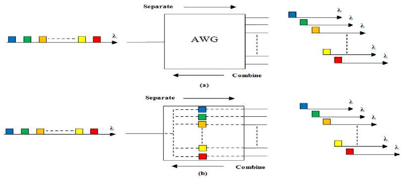
Fig. 1. Separation/combination of channels from/to a WDM set with an AWG (a), and illustration of the AWG as a bank of pass band filters (b).
The number of WDM channels that an AWG can handle, and their spacing, depends on the design of the device. The internal construction of an AWG is based in optical waveguides laid over a solid substrate. Hence, the AWG is an integrated-optic component belonging to the family of planar devices, known as Planar Light wave Circuits,
PLC. The waveguide arrangement is shown in Fig. 2. There are input waveguides that may be connected to fibers. The light at the input, formed by several wavelengths, is coupled to the arrayed waveguides by means of a slab coupler, which is also known as free propagation region.
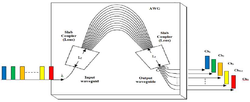
Fig. 2. AWG waveguide layout.
The arrayed waveguides have different lengths, specifically; the path length difference between adjacent waveguides is constant. The different wavelengths of the light experience different phase changes within the arrayed waveguides. The latter, combined with the second slab coupler, produces the spatial separation of the wavelengths composing the light incoming to the device [7].
-
III. M ODELING B ASICS AND A NALYSIS
-
III. 1. M ATERIALS BASED ARRAYED WAVEGUIDE GRATING A) P URE SILICA GLASS (S I O2) BASED MATERIAL The refractive index of this waveguide is cast under the Sellemier equation as the following [8]:
2 2-1 , A2 , A 3 2 , A 5 2
2 2 - A 2 2 2 - A 4 2 2 - A 6 2
The set of parameters is recast and dimensionally adjusted as: A 1 = 0.691663, A 2 =a 2 T; a 2 = (0.0684043/To), A 3 = 0.4079426, A4=a 4 T; a 4 = (0.1162414/T 0 ), A 5 = 0.8974794, and A 6 =a 6 T; a 6 = (9.896161/T 0 ). Where T is the temperature of the material in ºC, T 0 is the room temperature and is considered 25 ºC. Then the differentiation of Eq. (1) w. r. t operating wavelength λ yields:
dn = -2 n ) d 2
A 1 A 22 A 3 A 42 A 5 A 62
2 j2 2 + 2 j2 2 + 2 ? 2
( 2 - A 2 ) ( 2 - A 4 ) ( 2 - A 6 )
The differentiation of Eq. (1) w. r. t T gives:
dn _ L 2 / ) A i A 2 a 2 A 3 A 4 a 4 A 5 A 6 a 6
dT 11 . [ ( X 2 - A 2 2 ) 2 ( X 2 - A 4 ) 2 ( X 2 - A 2 ) 2
B) L ITHIUM NIOBATE (L I N B O 3 ) BASED MATERIAL
The refractive index of this waveguide is cast under the Sellemier equation as the following [9]:
n
= B i + B 2 M +
B з + B 4 M X - ( B 5 + B 6 M ) 2
B 7 + B 8 M
+ X 2 - B 9 2
- BWX 2(4)
The set of parameters is dimensionally adjusted as: B 1 =5.35583, B 2 =4.629x10⁻⁷, B 3 =0.100473, B 4 =3.862x10⁻⁸, B 5 =0.20692, B 6 = -0.89x10⁻⁸, B 7 =100, B 8 =2.657x10⁻⁵,
Where m is the diffraction order, λ is the operating wavelength, λ f is the final wavelength. The diffraction order is an important parameter. Once the diffraction order m is determined, some other parameters of the AWG device are also determined, such as the length difference of adjacent waveguides, focal length of the slab optical waveguide, free spectral range, maximum number of input/output wavelength channels, and number of the arrayed waveguides. The path length difference between adjacent arrayed optical waveguides ΔL is given by [12]:
^ L = m ^ 0 , (12) n
B 9 =11.34927, B 10 =0.015334, and M= (T-T o ). (T+570.82).
Equation (4) can be simplified as:
n
= B 12
+
B 34
X2
B 562
+
B 78
X2
B 92
B io X2
Where, n is the refractive-index of AWG, and λ 0 is the center wavelength of the arrayed waveguide in μm. The focal length of slab waveguide (L f ) is given by the following equation [12]:
Where B 12 =B 1 +(B 2 M), B 34 =B 3 +(B 4 M); B 56 =B 5 +(B 6 M), and B 78 =B 7 +(B 8 M). Differentiation of Eq. (5) w. r. t λ yields:
Lf =
ns d2 n m AX ng
d -(X] n ) dX v ’
B 34 B 78
2 + 2 + B io
( X 2 - B 562 ) 2 ( X 2 - B v
The differentiation of Eq. (5) w. r. t T gives: dn__ ( dM / dT ) Г t B 4 ( X 2 - B 562 ) + (2 B 6 B 34 B 56 ) + B 8
dT" 2 n [ 2 ( X2 - B 562 ) 2 ( X 2 - B 92 )
Where (dM/dT)=2T+(570.82-T o ).
Where n s is the effective index of the slab waveguide, d is the pitch length of adjacent input/output channels and arrayed waveguides in μm, Δλ is the wavelength channel spacing in nm, and n g is the group refractive index and is given as the following:
n g = n - ^ 0 dn , (14)
d X
C) G ALLIUM ALUMINUM ARSENIDE (G A (1- X )A L ( X )A S ) BASED MATERIAL
Parameters required to characterize the temperature and operating wavelength dependence of the refractive-index, where Sellmeier equation is under the form of [10]:
n 2 = C j + - C 2— - C X2 (8) X 2 - C 3
The set of parameters is recast and dimensionally adjusted as [8]: C 1 = 10.906-2.92x, C 2 = 0.97501, C 3 =c 3 T2; c 3 = (0.52886-0.735x/T o )2, for x < 0.36. And C 4 =c 4 (0.93721+ 2.0857x10⁻⁴T); c 4 =0.002467(1.14x+1).
Differentiation of Eq. (8) w. r. t λ gives:
An important property of the AWG is the free spectral range (FSR), also known as the demultiplexer periodicity. This periodicity is due to the fact that constructive interface at the output free spectral range or region can occur for a number of wavelengths. The free spectral range denotes the wavelength and frequency spacing between the maximum of the interface pattern because of the periodic characteristic of the AWG transfer function, and can be [12]:
FSR = ^ ^ n- , (15)
mng
The maximum number of I/O wavelength channels N max
depends on the FSR. The bandwidth of the multiplexed light, that is N max Δλ must be narrow than an FSR to prevent the overlapping of orders in the spectral region. Therefore, N max can be derived as follows [12]:
dn = - ( X n )
dX ' ’
C 2
( x2 - C з
+ C 4
The differentiation of Eq. (8) w. r. t T gives:
d- = 12 n ) dT
2 c 3 C 2 T
. ( x2 - C з P
- (2.0857 x 10 - 4 c 4 X 2)
N max
= int eger
III. 2. O PERATING PARAMETERS OF AWG
We expressed the corresponding grating order a function of operating wavelength range according to its band applications for a certain spectrum range as [11]:
X
m =----- X f - X
FSR
"A T J
The number of the arrayed waveguides P is not a dominant parameter in the AWG design because the
wavelength channel spacing AX and maximum number of
wavelength channels Nmax do not depend on it. Generally, P is selected so that the number of the arrayed waveguides is sufficient to make the numerical aperture
(NA), in which they form a greater number than the input/output waveguides, such that almost all the light diffracted into the free space region is collected by the
array aperture. As a general rule, this number should be bigger than four times the number of wavelength channels [13, 14]:
n „ f FSR i
P = 4int eger I-----I .
I A X J
-
IV. S IMULATION R ESULTS AND D ISCUSSIONS
We have investigated the new materials based arrayed waveguide grating optical devices for multi-band multiplexing/demultiplexing applications. In fact, the employed software computed the variables under the following operating parameters, for temperature variations from T=25 ºC to T=65 ºC. and also under different channel spacing ∆ λ =0.4 nm and ∆ λ =0.2nm.
Table1. Typical values of operating parameters in proposed model [13].
|
Operating parameter |
Symbol |
Value |
|
Final wavelength |
λ f |
1.65 μm |
|
Center wavelength |
λ 0 |
1.55 μm |
|
Pitch length |
d |
15 μm |
|
Slab refractive-index |
n s |
3.06 |
-
A) Variations of the diffraction order
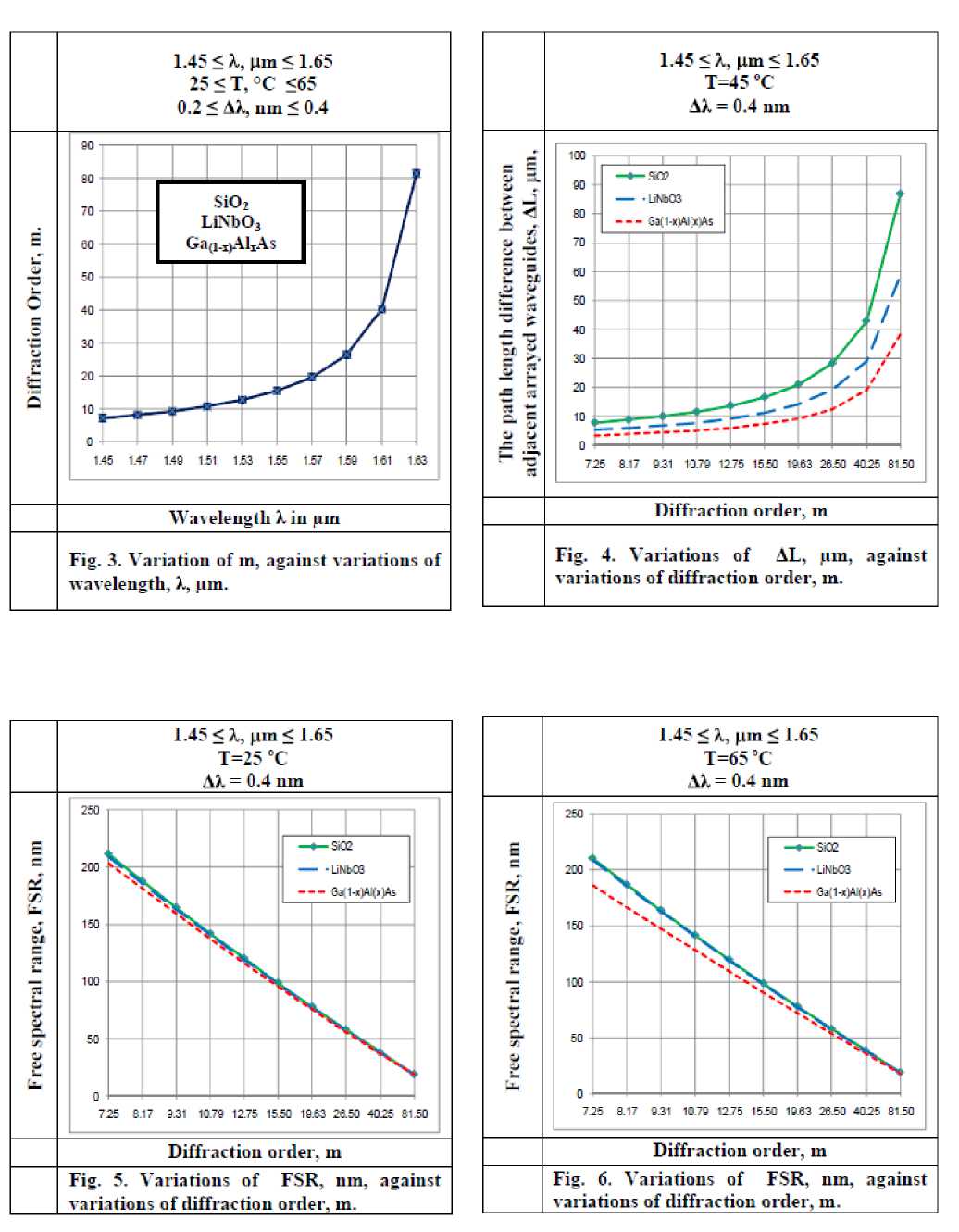
Variations of the diffraction order m are investigated against variations of the controlling set of parameters as displayed in Fig. 3 for all materials used in our research (SiO 2 , LiNbO 3 ,Ga (1 -x ) AlxAs). This figure clarifies that while operating wavelength λ increases, this leads to diffraction order m also increases at the assumed set of the operating parameters.
-
B) Variations of the path length difference between adjacent arrayed waveguides
Variations of ΔL are investigated against variations of the controlling set of parameters as displayed in Fig. 4 for all material used in our research (SiO2, LiNbO3, Ga ( 1-x ) AlxAs ). This figure clarifies the following results:
-
i. As diffraction order m increases this results in path length difference ΔL also increases for all materials based conventional AWG.
-
ii. For certain value of diffraction order m, the value of path length difference ΔL for SiO 2 is the largest than LiNbO 3 and Ga (1 -x ) AlxAs.
C)Variations of the free spectral range
Variations of FSR, are investigated against variations of the set of parameters as displayed in Figs. (5, 6) for all materials used in research (SiO 2 , LiNbO 3 , Ga (1-x) Al x As ). These figures clarify the following results:
-
i. As diffraction order m increases, FSR decreases for all materials based conventional AWG.
-
ii. For certain value of diffraction order m, value of FSR for SiO 2 is larger than LiNbO 3 and Ga(1-x)AlxAs.
-
iii. As ambient temperature T increases, FSR decreases for all materials, but in the case of using Ga(1-x)AlxAs there was significant decreasing.
-
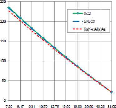
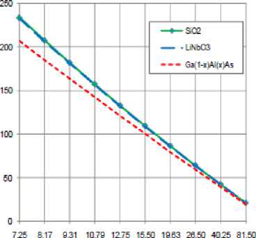
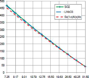
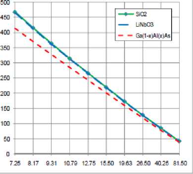
D) Variations of the path focal length of slab waveguide
Variations of path focal length L f , are investigated against variations of the controlling set of parameters as displayed in Figs. (7-10) for all material used in our research (SiO 2 , LiNbO 3 , Ga (1 -x ) AlxAs ). These figures clarify the following results:
-
i. As diffraction order m increases, this results in decreasing of path focal length of slab waveguide for all materials based conventional AWG.
-
ii. For certain value of diffraction order m, value of path focal length of slab waveguide for SiO 2 is the largest than LiNbO 3 and Ga (1 -x ) AlxAs.
-
iii. As ambient temperature T increases, this leads to decrease in path focal length for all materials, but in the case of using Ga (1 -x ) AlxAs there was significant decreasing.
-
iv. As channel spacing Δλ decreases, this results in increasing path focal length of slab waveguide for all materials based conventional AWG.
-
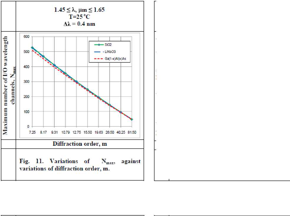
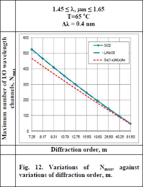
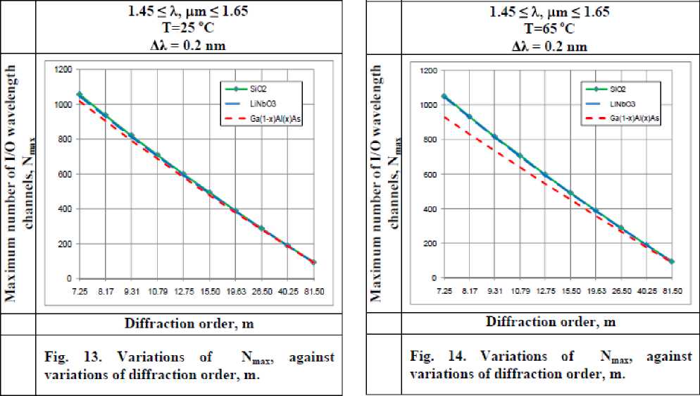
E) Variations of maximum number of I/O wavelength channels
Variations of Nmax, are investigated against variations of the assumed set of parameters as displayed in Figs. (11-14) for all materials based conventional AWG devices in our research (SiO 2 , LiNbO 3 , Ga (1 -x ) AlxAs). These figures clarify the following results:
-
i. As diffraction order m increases, this results in maximum number of trans mitted channels Nmax decreases for all materials based conventional AWG devices.
-
ii. For certain value of diffraction order m, SiO 2 based AWG presents the largest number of transmitted channels than LiNbO 3 and Ga (1 -x ) AlxAs.
-
iii. As ambient temperature T increases, this leads to decrease in number of transmitted channels N max for all materials, but in the case of using Ga (1-x) Al x As, there was significant decreasing.
-
iv. As channel spacing Δλ decreases, this results in increasing number of transmitted channels for all materials based conventional AWG.
-
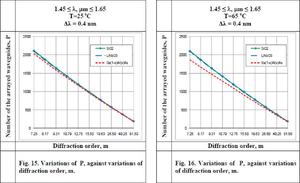
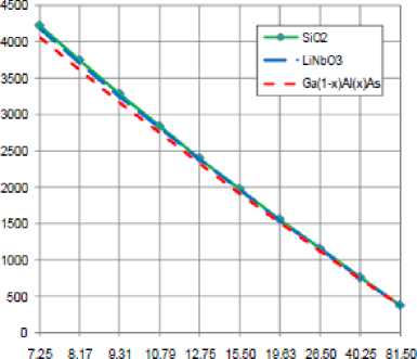
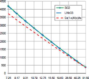
F) Variations of number of the arrayed waveguides
Variations of P, are investigated against variations of the controlling set of parameters as displayed in Figs. (15-18) for all materials used in our research (SiO 2 , LiNbO 3 , Ga (1 -x ) AlxAs). These figures clarify the following results:
-
i. As diffraction order m increases, this leads to decrease in number of arrayed waveguides for all used materials.
-
ii. For certain value of diffraction order m, number of arrayed waveguides for SiO 2 is the largest than LiNbO 3 and Ga (1-x) Al x As
-
iii. As ambient temperature T increases, this results in decreasing number of arrayed waveguides for all materials, but in case of using Ga (1-x) Al x As there was significant decreasing.
1.45
25 < Т, °C <65 0.2 < АХ, nm < 0.4
Wavelength X in pm
1.45 < X, pm < 1.65 T=25 °C AX = 0.4 nm
Diffraction order, m
1.45 < X, pm < 1.65 T=65 °C ЛХ = 0.4 nm
Diffraction order, in
45 1.47 1.49 151 153 1.55 157 159 1.61 1.63
725 8.
17 9.;
31 1079 12
—•—ЗЙ2
--- -LiNbOB
---6a;l-x|A.(x|As
.75 1550 19.63 26.50 4025 81
17 931 10.78 12.
75 1550 19 53 25.50 4025 8150
SiO2 LLNbO3 Gap-yAhAs
0 725 8.
—•—see
--- -LiNbOB
---Ga(1-x)AjpiAs
1.45
ДХ = 0.4 nm
Diffraction order, m
725 8.17 931 10.79 12.75 1550 19.63 26.50 4025 8150
Fig. 4. Variations of AL, pm, against variations of diffraction order, m.
—•—see
— -иньоз
---Ga(1-*)AI(x)As
Fig. 3. Variation of m, against variations of wavelength, X, pm.
Fig. 5. Variations of FSR. nm, against variations of diffraction order, m. __________
Fig. 6. Variations of FSR, nm, against variations of diffraction order, m. __________

SiO
Лк = 0.4 nm
1.45 < к, pm <1.65
Diffraction order, m.
Fig. 19. Variations of refractive index n, against variations of diffraction order, in.
Лк = 0.4 nm

1.45 < к, pm <1.65
Ga^Aln^yAs
Diffraction order, m.
Fig. 21. Variations of refractive index n, against variations of diffraction order, m.
|
£7*4^ |
||||||||||||
|
= 1 .45 pm = 1 .55 pm = 1 .65 pm |
||||||||||||
|
•--- --- А |
||||||||||||
iv. As channel spacing Δλ decreases, this leads to increase number of arrayed waveguides for all use materials.
-
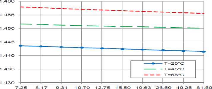
G) Variations of the refractive index
Variations of refractive-index n, are investigated against variations of the controlling set of parameters as displayed in Figs. (19-21) for all materials based conventional AWG devices (SiO 2 , LiNbO 3 , Ga (1 -x ) AlxAs). These figures clarify the following results:
-
i. As diffraction order m increases, refractive index n decreases for all used materials.
-
ii. For certain value of diffraction order m and ambient temperature T, the refractive index n for SiO 2 is the lowest than LiNbO 3 and Ga (1 -x ) AlxAs.
-
iii. As ambient temperature T increases, refractive index n increases for all materials based conventional AWG.
-
H) Variations of dn/dT
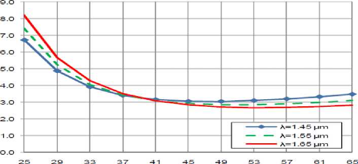
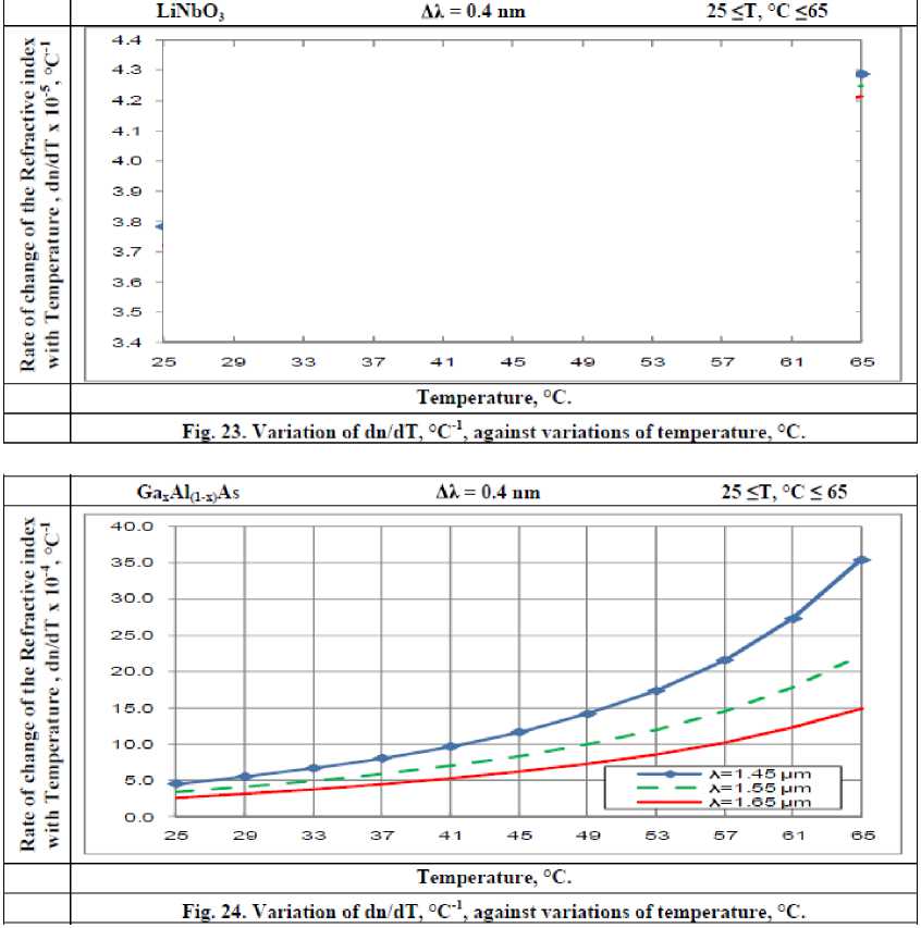
Variations of dn/dT are investigated against variations of the controlling set of parameters as displayed in Figs. (22-24) for all materials based conventional AWG devices (SiO 2 , LiNbO 3 , Ga (1 -x ) AlxAs). These figures clarify the following results:
-
a) Within the effect of ambient temperature:
-
i. For SiO 2 : As ambient temperature T increases, rate of change of refractive-index with respect to temperature dn/dT decreases exponentially until reach to approximate value of 39 °C, as well as there is slightly decreasing until reaches to approximate value of 51 °C, and after that there is exponential increasing.
-
ii. For LiNbO 3 : As ambient temperature T increases, rate of change of refractive-index with respect to temperature dn/dT increases linearly.
-
iii. For Ga(1-x)AlxAs: As ambient temperature T increases, rate of change of refractive-index with respect to temperature dn/dT increases
exponentially.
b)Within the effect of wavelength at certain temperature:
-
i. For SiO2: As operating signal wavelength λ increases, dn/dT also increases exponentially until reaches to approximate value of 39 °C , and after that as λ increases, dn/dT decreases exponentially.
-
ii. For both LiNbO 3 & Ga (1 -x ) AlxAs: As operating wavelength λ increases, dn/dT decreases.
-
V. Conclusions
In a summary, we have investigated the ultra wide wavelength multiplexing/demultiplexing conventional AWG for multi band applications. It is observed that the increased diffraction order, the decreased refractive index for all materials based AWG devices. We have indicated that the increased of both ambient temperature and diffraction order, the decreased number of arrayed waveguides. As well as the decreased of ambient temperature, channel spacing, and diffraction order, this results in increasing of number of input/output wavelength channels. Moreover we have observed that SiO2 based material for AWG devices presents the highest number of transmitted channels than the other materials based conventional AWG. So SiO2 material based for conventional AWG is the best candidate for core material than the other materials used in our research.
References Ultra Wide Wavelength Multiplexing/Demultiplexing Conventional Arrayed Waveguide Grating (AWG) Devices for Multi Band Applications
- Abd El-Naser A. Mohammed, Gaber E. S. M. El-Abyad, Abd El-Fattah A. Saad, and Ahmed Nabih Zaki Rashed, “High Transmission Bit Rate of A thermal Arrayed Waveguide Grating (AWG) Module in Passive Optical Networks,” IJCSIS International Journal of Computer Science and Information Security, Vol. 1, No. 1, pp. 13-22, May 2009.
- H. Kosek, Y. He, X. Gu, and X. Fernando, “All Optical Demultiplexing Closely Spaced Multimedia Radio Over Fiber Signals Using Subpicometer Fiber Bragg Grating,” Journal of Lightwave Technology, Vol. 13, No.4, pp. 191-200, 2006.
- J. Ma, J. Yu, C. Yu, X. Xin, J. Zeng, and L. Chen, “Fiber Dispersion Influence on Transmission of the Optical Millimeter Waves Generated Using LN-MZM Intensity Modulation,” J. of Ligthwave Technol., Vol. 25, No. 2, pp. 3244–3256, 2007.
- Yang, Y., C. Lou, H. Zhou, J. Wang, and Y. Gao, “Simple pulse compression scheme based on filtering self-phase modulation broadened spectrum and its application in an optical time-division multiplexing systems,” Appl. Opt., Vol. 45, 7524–7528, 2006.
- S. Sawetanshumala, and S. Konar, “Propagation of a mixture of Modes of A laser Beam in A medium With Securable Nonlinearity,” Journal of Electromagnetic Waves and Applications, Vol. 20, No. 1, pp. 65–77, 2006.
- R. Gangwar, S. P. Singh, and N. Singh, “Soliton Based Optical Communication,” Progress In Electromagnetics Research, PIER Vol. 74, No.3, pp. 157–166, 2007.
- A. Sangeetha , S. K. Sudheer, and K. Anusudha, “Performance Analysis of NRZ, RZ, and Chirped RZ Transmission Formats in Dispersion Managed 10 Gbit/sec Long Haul WDM Lightwave Systems,” International Journal of Recent Trends in Engineering, Vol. 1, No. 4, pp. 103-105, May 2009.
- ITU-T, series G, “General aspects of optical fiber cable,” pp. 10-11, 2009.
- D. H. Jundt, “Temperature-dependent Sellmeier equation for the index of refraction, ne, in congruent lithium niobate,” Optics Letters, Vol. 22, No. 20, pp.1553-1555, 1997.
- Osama A. Oraby, “Propagation of An Electromagnetic Beams in Nonlinear Dielectric Slab Wave Guides,” Minufiya Journal of Electronic Engineering Research, Vol. 16, No. 1, pp. 27-44, 2006.
- J. Qiao, F. Zhao, J. W. Horwitz, R. T. Chen, and W. W. Morey “A thermalized Low Loss Echelle Grating Based Multimode Dense Wavelength Division Multiplexer,” J. Applied Optics, Vol. 41, No. 31, pp. 6567-6575, 2002.
- Abd El-Naser A. Mohammed, Abd El-Fattah A. Saad, and Ahmed Nabih Zaki Rashed, “Matrices of the Thermal and Spectral Variations for the fabrication Materials Based Arrayed Waveguide Grating Devices,” International Journal of Physical Sciences, Vol. 4, No. 4, pp. 205-211, April 2009.
- Abd El-Naser A. Mohammed, Abd El-Fattah A. Saad, and Ahmed Nabih Zaki Rashed, “Estimated Optimization Parameters of Arrayed Waveguide Grating (AWG) for C-Band Applications,” International Journal of Physical Sciences, Vol. 4, No. 4, pp. 149-155, April 2009.
- Abd El-Naser A. Mohammed, Abd El-Fattah A. Saad, and Ahmed Nabih Zaki Rashed, “Thermal Sensitivity Coefficients of the Fabrication Materials Based A thermal Arrayed Waveguide Grating (AWG) in Wide Area Dense Wavelength Division Multiplexing Optical Networks,” International Journal of Engineering and Technology (IJET), Vol. 1, No. 2, pp. 131-139, June 2009.
