Design of Fast Pipelined Multiplier using Modified Redundant Adder

Author: Rakesh Kumar Saxena, Neelam Sharma, A. K Wadhwani
Journal: International Journal of Intelligent Systems and Applications(IJISA) @ijisa
Article in issue: 4 vol.4, 2012.
Free access
Carry free arithmetic using higher radix number system such as Redundant Binary Signed Digit can be used to meet the demand for computers operating at much higher speeds. The computation speed can also be increased by using the suitable design of adder and multiplier circuits. Fast RBSD adder cells suggested by Neelam Sharma in 2006 using universal logic are modified in the proposed design by reducing the number of gates. Due to reduction in gate count, number of gate levels and hence the circuit complexity is also reduced. As multiplication is repetitive addition, the implementation time of the multiplier circuit will also be reduced to a great extent by using modified design of adder cell to add the partial products. These partial products are added using pipelined units to reduce implementation time further. Thus with the use of proposed RBSD adder, other arithmetic operations such as subtraction, division, square root etc. can be performed much faster. It is concluded that efficiency of the proposed RBSD adder and multiplier is improved as compared to the techniques conventionally used in high speed machines. Thus the proposed modified RBSD adder cell using universal gates can be used to design fast ALU with many additional advantages.
Signed Digit, Fast Multiplier, Fast Computing, High-speed arithmetic, Pipelining.
Short address: https://sciup.org/15010243
IDR: 15010243
Text of the scientific article Design of Fast Pipelined Multiplier using Modified Redundant Adder
Published Online April 2012 in MECS
-
I. INTRODUCTION
The circuits for arithmetic operations like adder and multiplier have long propagation time delay, limited range of bits and complexity in hardware. RBSD numbers is gaining much attention due to carry free addition property and thus fast addition[1,2]. The computation time also depends upon the suitable circuit design[3]. Therefore it is highly desirable to construct efficient digital logic circuit. In 2006, N. Sharma proposed the adder cell design using universal logic gates for fast
addition[5]. In this paper the adder cells are modified and which further used for the computation of high speed adder and multiplier circuit.
Multiplication is the repetitive addition of the partial products[6,7]. The partial products generated can be reduced by applying RBSD booth’s encoding technique [8]. The concept of pipelining is desirable to speed up the operation[9,10]. Therefore for the fast multiplication, reduced number of partial products are added simultaneously using proposed adder cell structure and addition is carried out in pipelined structure due to which the entire ALU operation can be fast.
This paper emphasizes briefly about the RBSD addition in section 2. The concept of fast adder cell using universal logic is described in the sections 3. Section 4 gives comparison among the previous and proposed cell structures. An implementation and comparison between CLA and RBSD adder upto 64 bit is made in section 5. Idea to design fast multiplier with the concept of pipelining is given in section 6. Finally in section 7 implementation and comparison of Wallace Booth Multiplier (WBM) and pipelined RBSD Multiplier is presented.
-
II. RBSD Addition
Avizienis[1] in 1961 proposed RBSD number system in which the digit set (1, 0, 1 ) is used to represent numbers. The decimal value of RBSD number can be calculated by following relation.
Let the number (10)10 can be represented in binary as
1010 while in RBSD it can be represented by more than one way i.e. 1 1 1 1 0 or 1 1 0 11 0. These redundant representations of numbers gives technique of carry free arithmetic.
Adder is the basic building block for the computation of all mathematical operations. Hence a carry free addition technique is desirable which achieved using following equations[1].
These equations 2-4 gives the result of addition in three steps. There was no carry propagation chain as at the last stage of computation the digit w i ’’ and t i ’’ both never 1 or 1 simultaneously. A number of any bit length can be added in constant time period.
The digital systems do not support the -1 logic therefore for the logic circuit design of RBSD Adder, Kal
|
and Rajashekhar, 1990 has given following Boolean expressions 5-9[11]. |
|
d i = m , ®_ X i+ X i" ® y i+ yf (5) |
|
m i+1 = x i + y i+ (6) |
|
b i+1 = m i x i+ x i- + x i+ y i+ + y i+ y i- m i |
|
+ x i+ x i- y i+ y i- (7) |
|
s i+ = d i _ b i (8) |
|
s i- = d i b i (9) |
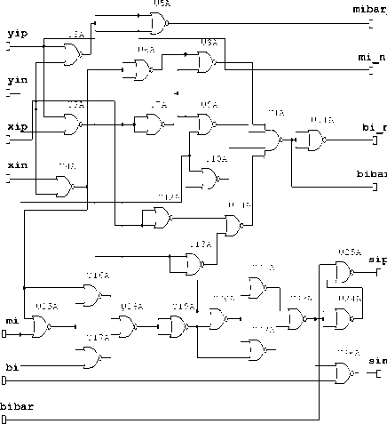
Figure 1. RBSD Adder Cell: NOR-NOR Logic
Here m i , b i and d i are binary variables with digit set {0,1} and xi + xi - , yi + yi - are RBSD input numbers and si + si - output sum in RBSD with digit set (-1,0,1) represented by binary encoded form i.e. (0,1), (0,0), (1,0) respectively.
-
III. Fast Adder Design
N Sharma et. al. in 2006 designed the adder cells by
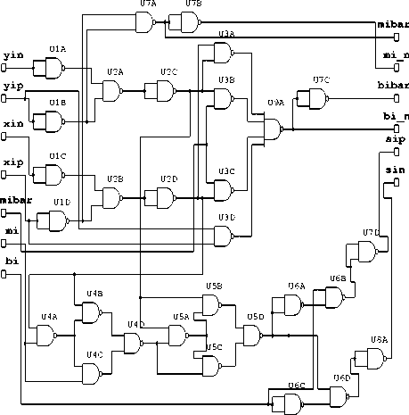
Figure 2. RBSD Adder Cell: NAND-NAND Logic.
TABLE I. variable used
Proposed Adder Cell design
A modification has been made in the architecture of universal logic adder cell structure by reducing the gate count. The reduction in gate count is due to redesign of part of the circuit which is giving intermediate output d i . This output is produced through XOR gate as given in equation 5.
If A, B, C are the input bits and Y is output then the logic equation for 3-input XOR gate will be
Y = A ⊕ B ⊕ C
(Let A, B, C input and Y output)
=
The above logic equation can be implemented using 4 AND and 1 OR gate. This logic equation can also be implemented using either 6 NOR gates or 5 NAND gates by replacing equivalent universal logic implementation of
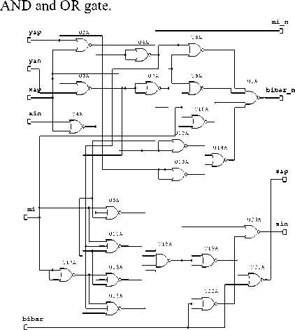
Figure .3. Modified Cell: NOR-NOR logic and after 2 logic levels as shown in fig 4. One more NAND gate is reduced due to no need of signal mi_n for further stages in modified design.
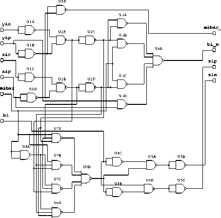
Figure 4. Modified Cell: NAND-NAND logic
Hence the output d i produced by 3-input XOR gate have been achieved after 10 NOR gates (U15A to U24A) and passing the signal over 8 logic levels in the adder cell designed by N Sharma using NOR-NOR logic as shown in figure 1. But in proposed modified design the same output can be achieved using 6 NOR gates (U5A, U11A, U15A, U16A, U18A and U19A) only and crossing the 3 logic levels as shown in fig 3 [4]. Similarly the output di in NAND-NAND adder cell proposed by N Sharma shown in fig. 2 has been achieved after 8 NAND gates (U4A, U4B, U4C, U4D, U5A, U5B, U5C & U5D) and passing the signal over 7 logic levels. But in proposed modified design the same output can be achieved using five NAND gates (U7A, U7B, U7C, U8A & U6B) only Hence the Modified adder cell has been designed using reduced number of NOR or NAND gates.
-
IV. Comparison of various Adder Cell
Hardware
Figure 5 and Table II shows a clear comparison among the circuit shown in figure 1, 2, 3 and 4. It is clear that the modified architectures are better as the numbers of inputs are less as compared to other cell structures. Further the number of gates required in proposed designs is also less. To get the final output, the input crosses less levels in proposed design.
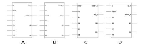
Figure 5. Block diagram representation of adder cell (A) NOR-NOR (B) NAND-NAND (C) modified–NOR (D) modified-NAND
T able II. C omparative A nalysis among various adder cells
|
Type of Adder Cell |
Total NOR / NAND Gate used |
Required I/P Signals |
Levels Crossed to get O/P |
|
|
si + |
s i- |
|||
|
NOR-NOR |
26 |
7 |
9 |
8 |
|
Modified NOR-NOR |
22 |
6 |
6 |
6 |
|
NAND-NAND |
30 |
7 |
11 |
10 |
|
Modified NAND-NAND |
26 |
6 |
8 |
8 |
Simulation Result
All the modified Adder cell architectures are verified using Multisim software and their timing reports are generated on Xilinx project navigator.
T able III. T ime D elay
|
RBSD Adder Cell Type |
Time Delay (ns) |
|
NOR-NOR |
11.861 |
|
Modified NOR-NOR |
11.807 |
|
NAND-NAND |
11.978 |
|
Modified NAND-NAND |
11.861 |
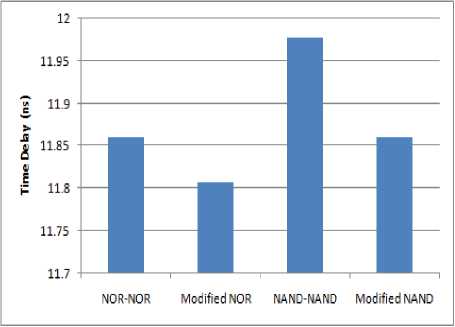
Figure 6. Time delay in different architectures of Adder cell
The FPGA implementation of these circuits is made on Spartan II XC2S50-5pq208. It is clear from the table III and figure 6 that the propagation delay time to get the addition result for one bit addition is less in modified architectures as compared to previous.
-
V. Implementation of CLA and modified RBSD Adder
In this section the VHDL implementations of Carry Look Ahead (CLA) Adder[12] and RBSD adder of n-bit is simulated on modelsim simulator and synthesized on xilinx project navigator and their timing reports were observed for various values of n up to 64 bits.
A comparative graph between CLA and RBSD adder is shown in figure 7. It is observed that the delay produced in RBSD adder is high compared to CLA initially as the number of bits are less but as the number of bits increases CLA adder takes more time but in RBSD time remains constant which is very less for any number of bit additions. In CLA the add time increases gradually due to logic for carry calculation and hence hardware circuit changes with increase in bits.
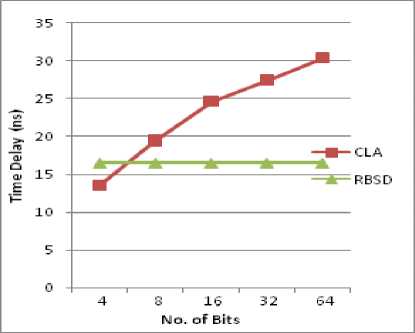
Figure 7. Timing comparison among CLA and Modified RBSD Adder
Hence for higher bit length, RBSD adders are suitable due to carry free addition and same adder cell structure is used for the addition of any bit number.
-
VI. Fast Multiplier Design
Multiplication is the most critical operation in every computational system. It is the repetitive addition of partial products. It involves two basic operations [7].
-
1. The generation of partial products
-
2. Their accumulation to produce the final product.
Hence for speeding up the multiplication process firstly there should be reduction in number of partial products generated which can be achieved by Booth’s encoding technique [6,8]. Secondly the time needed to add these partial products which can be achieved by using the carry free SD pipelined adders. This approach reduces the delay time immensely instead of carry save adder. The steps for multiplication are detailed below. Take two binary numbers one multiplicand and other multiplier.
-
1. Convert the multiplicands from two’s complement form to RBSD representation (multiplier is retained in two’s complement form).
-
2. Generate n/2 RBSD partial products using Booth’s bit-pair recoding technique on the n-bit two’s complement multiplier and the RBSD multiplicand.
-
3. Add the partial products pair wise by means of a binary tree of log 2 (n/2) levels of RBSD adders.
-
4. Convert the resulting RBSD product into two’s complement form.
As per the steps the multiplicand is converted into two’s compliment form and then to RBSD form. Multiplier is also converted to 2’s compliment form and then the partial products are generated as per Booth Bit pair recoding technique.
The partial products are added simultaneously using RBSD adders to generate the partial product sums. Log2 (n/2) levels of RBSD adders are required to obtain the product in RBSD. Finally the product is converted to 2’s compliment form using CLA adder.
Pipelined design
The 16 x 16 fixed-point multiplication units can be divided into six pipeline stages as shown in figure 8. Stage S1 generates the partial product and stage S2 converts the partial products to RBSD numbers. Stages S3, S4 and S5 add the RBSD numbers. Here it is important to note that since RBSD adder delay time is independent of word length with increased complexity, stages S3, S4 and S5 will have the same delay time. Stage S6 is a CLA adder used to convert the RBSD number in two’s complement form.
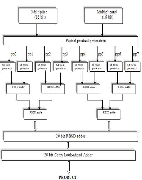
Figure 8. Block Diagram for multiplication of 16 x 16 bits.
Delay times of stages S1, S2 and S6 can be further adjusted. The pipeline is thus divided into six stages and the clock rate can be fixed as desired to give appropriate results. The pipeline unit for 16x16 bit multiplication is shown in figure 8. Fast addition techniques i.e. Booth’s encoding, addition of partial product using modified cell and pipelining will help in increasing the processing speed [9],[14].
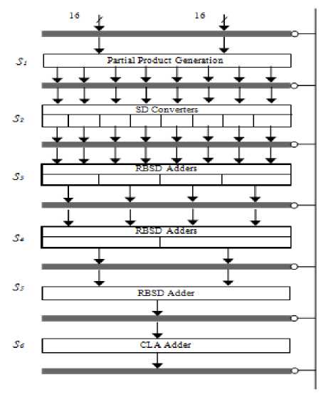
Figure 9. Pipeline unit for fixed-point multiplication of 16x16 bit numbers.
-
VII. Implementation and timing analysis of Pipelined multiplier with WBM
Pipelined RBSD multiplier and Wallace Booth multiplier (WBM) upto 16x16 bit length was simulated and synthesized using VHDL. The software used for simulation was FPGA Advantage and that for synthesis was Xilinx Project Navigator.
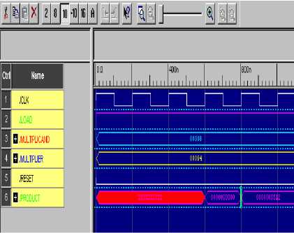
Figure 10. Simulation Result of Pipelined Multiplier Comparison of WBM and RBSD multiplier
Simulation output after multiplication is shown in figure 10 and timing analysis between WBM and RBSD Multiplier is shown in figure 11. The working of multiplier is also verified using field programmable gate array XC2S50-5pq208.
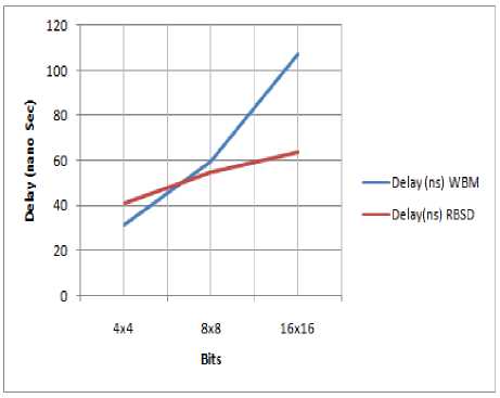
Figure 11. Comparison between WBM and RBSD Multiplier
-
VIII. Conclusion
The delay time of the adder cell has been reduced in the modified architectures using NOR-NOR logic and NAND-NAND logic. The number of gate counts has been reduced in the proposed adder cell and hence overall reduction in number of logic levels and inputs will also reduce the circuit complexity.
The efficiency of RBSD adder increases as bit length of the summands increases. The higher the bit length, the efficiency of RBSD adder is high as compared to CLA. The delay time of RBSD multiplier is reduced using the pipelined design and fast RBSD adder cell for the addition of partial products. It is concluded that delay time of multiplication is less in RBSD multipliers as compared to Wallace Booth Multiplier and verified by the result of synthesis due to carry free addition using modified adder cell and pipelining.
Finally addition is the base for all the mathematical operations[13],[15],[16] like division, reciprocation, square rooting, inverse square rooting etc., fast arithmetic processor of higher bit length can be designed using proposed architectures of adder cell. Therefore the proposed modified RBSD adder cell is highly appreciable for the design of ALU of higher bit length. The new designs will be simpler, fast and will consume less power.
References Design of Fast Pipelined Multiplier using Modified Redundant Adder
- Avizienis A., “Signed digit number representation for fast parallel arithmetic,” IRE Trans. Electron Computers., vol EC-10, pp.389-400, 1961.
- Hwang K., “Computer Arithmetic/Principles, Architecture and Design,” New York: Wiley, 1979.
- Chow C. Y. and Robertson J. E., “Logical Design of a Redundant Binary Adder,” In Proc. of 4th Symposium on Computer Arithmetic, pp. 109-115, 1978.
- Rakesh Kumar Saxena, Neelam Sharma and A. K. wadhwani, “Novel Design of Fast RBSD Adder with Reduced NOR-NOR Logic”, International Journal of Computer and Network Security(IJCNS), vol. 2, no. 7, pp 52-56 (2010).
- Neelam Sharma., “Development of Fast RBSD Arithmetic Logic Unit”, Ph.D Thesis, U. P. Technical University, Lucknow, India, 2006.
- A. D. Booth.. “A Signed Binary Multiplication Technique,” J . mech. appl. math: 4, Oxford University Press, pp. 236-240, 1951.
- Chen, I Shi E. and Rajashekhara, T.N., “A fast multiplier Design Using Singed Digit Numbers and 3-Valved Logic,” In proc. of IEEE, Binngamton New York, 1991.
- Besli, N. and Deshmukh, R.G., “A novel Redundant Binary Signed–Digit (RBSD) Booth’s Encoding,” In proc. of IEEE, Southeastcon, 2002.
- Dadda L. and Piuri V., “Pipelined Adders,” IEEE Transactions on Computers, vol. 45, No. 3, pp. 348-356, 1996.
- Hallin, T. G. and Flynn M. J., “Pipelining of Arithmetic Functions”, IEEE Transactions of computers, pp. 880-885, 1972.
- Rajashekhar, T.N.and Kal, O., “Fast Multiplier Design using Redundant Signed- Digit Numbers”, International Journal of Electronics, vol.69, no. 3, pp –359-368, 1990.
- Gloria A. D. and Olivieri M., “Statistical Carry Look-ahead Adders,” IEEE Transactions on Computers, vol. 45, No. 3, pp. 340-356, 1996.
- Cortadella J. and Lang T., “High Radix Division and Square – Root with Speculation,” IEEE Transactions on Computer, vol. 43, no. 8, pp. 919-931, 1994.
- Jump J. R. and Ahuja S. R., “Effective Pipelining of Digital System,” IEEE Transaction on computers, vol. C-27, no. 9, pp. 855-865, 1978.
- Cotolora, S. and Vassiliadis, S. (2000). “Signed Digit Addition and Related Operations with Threshold Logic,” IEEE Transaction on Computers, vol. 49, no. 3, 2000.
- M D Ercegovac, J M Muller, Tisseran., “Reciprocation, Square root, Inverse Square root and some Elementary functions using small Multipliers”, IEEE Transactions on computers, vol 49, no. 7, July 2000.
- Parhami B, “Carry free Addition of Recorded Binary Signed-Digit Numbers,” IEEE Transactions on computers, vol. 37 no. 11, pp. 1470-1476 ,1988.
- Rajashekhar, T.N. and I-Shi Eric Chen., “A Fast Adder Design Using Signed-Digit Numbers and Ternary Logic,” In proc. IEEE Southern Tier Technical Conference, Binngamton, New York, pp.187-194, 1990.
