High Accuracy Swin Transformers for Image-based Wafer Map Defect Detection

Author: Thahmidul Islam Nafi, Erfanul Haque, Faisal Farhan, Asif Rahman
Journal: International Journal of Engineering and Manufacturing @ijem
Article in issue: 5 vol.12, 2022.
Free access
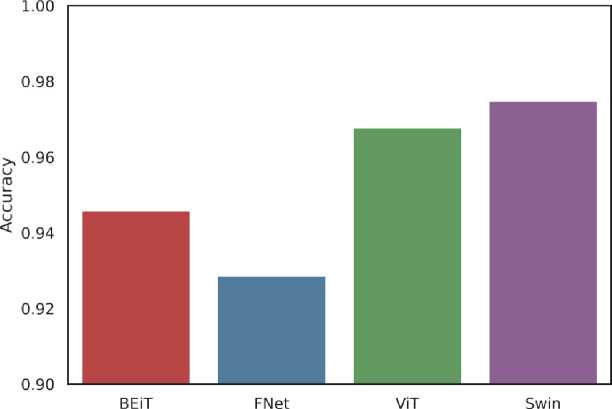
A wafer map depicts the location of each die on the wafer and indicates whether it is a Product, Secondary Silicon, or Reject. Detecting defects in Wafer Maps is crucial in order to ensure the integrity of the chips processed in the wafer, as any defect can cause anomalies thus decreasing the overall yield. With the current advances in anomaly detection using various Computer Vision Techniques, Transformer Architecture based Vision models are a prime candidate for identifying wafer defects. In this paper, the performance of Four such Transformer based models – BEiT (BERT Pre-Training of Image Transformers), FNet (Fourier Network), ViT (Vision Transformer) and Swin Transformer (Shifted Window based Transformer) in wafer map defect classification are discussed. Each of these models were individually trained, tested and evaluated with the “MixedWM38” dataset obtained from the online platform, Kaggle. During evaluation, it has been observed that the overall accuracy of the Swin Transformer Network algorithm is the highest, at 97.47%, followed closely by Vision Transformer at 96.77%. The average Recall of Swin Transformer is also 97.54%, which indicates an extremely low encounter of false negatives (24600 ppm) in contrast to true positives, making it less likely to expose defective products in the market.
Wafer defects, Transformer models, Machine learning, Swin transformer model
Short address: https://sciup.org/15018591
IDR: 15018591 | DOI: 10.5815/ijem.2022.05.02
Text of the scientific article High Accuracy Swin Transformers for Image-based Wafer Map Defect Detection
In semiconductor manufacturing, a wafer is a fundamental unit. A single wafer can accommodate hundreds or thousands of integrated circuits (ICs) [1]. The typical defect patterns (e.g., ring, scratch, semicircle, repeat, cluster) on wafer maps generally connect the possible causes of failure or process variations. As a result, major efforts in the semiconductor industry and academics have been made in recent decades to build high-performance fault detection and classification (FDC) models that can detect wafer defects early in the semiconductor fabrication process [2]. Various machine learning algorithms, which may be split into unsupervised and supervised learning categories, have been successfully applied in the detection and recognition of wafer map defects in recent years. Until recently, approaches involving supervised learning mostly included architectures with convolutional neural networks (CNN). CNNs are useful for automatic extraction of features from images. This is achieved by using a combination of kernels of varied dimensions and different kinds of pooling layers (Avg. pooling, Max pooling etc.). The kernels are responsible for extracting features in different regions or sub-sections of the image and for finding multiple distinct features even in the same location of an image. Feature summarization or localizing the most prominent features is performed by the pooling layers.
Although CNN architectures perform well in feature extraction, it becomes more computationally expensive to capture long-range dependencies in images with them. This is because filter size needs to be increased drastically to cover larger sections of an image. This also, in turn, decreases the statistical efficiency of the model. Transformers excel in this regard because of the presence of self-attention blocks in them. Transformers capture the interactions among the elements of a sequence for structured prediction problems. To update each component of a sequence, a self-attention layer accumulates global information from the entire input sequence [3]. Since the information from the entire image sequence is used for each component, the feature maps contain data even on very distant sub-segments of the image. As multiple attention heads are used, the aspect of capturing different features from the same region of the image is also preserved.
The main aim of this paper is to find the most suitable method for identifying wafer defects in wafer map using some prominent Transformer Architecture based vision models. Four transformer based models namely BEiT (BERT Pre-Training of Image Transformers) , FNet (Fourier Network), ViT (Vision Transformer) and Swin Transformer (Shifted Window based Transformer) are deployed on “MixedWM38” wafer dataset to propose the model with best accuracy for wafer defect detection.
The remainder of this paper is organized as follows:
The second section comprises Literature Review, third section discusses about data collection and methodology, the fourth section explains the experimental results and finally fifth section comprises the conclusion.
2. Literature Review
Over the years, semiconductor industry made significant improvements for developing high performance fault detection and classification machine learning models to detect wafer faults in semiconductor fabrication process.
Hoyeop Lee, Youngju Kim, Chang Ouk Kim [6] used a deep learning algorithm called stacked denoising autoencoder (SdA) for fault detection and classification of wafer faults. The dataset collected from work-site photolithography tool was used in the experiment and compared with twelve other models along with the proposed SdA’s classification method. The accuracy was 14% higher than the other compared models for wafer fault detection. In [7] authors classified surface defects that were visible in semiconductor wafers using vision-based machine learning method where four types of surface defects namely center, random, scrape and local were identified using convolutional neural networks. The experiment avoided using any refinement yet reached 98% to 99% accuracy and showed superior performance in contrast to the other implemented machine learning methods. Po-Chou Shih, Chun-Chin Hsu and Fang-Chih Tien [8] proposed deep learning neural network methods to determine the defects in wafer. Three powerful neural networks namely multilayer perceptron (MLP), convolutional neural network (CNN) and Residual neural network (ResNet) were implemented on wafer dataset and then compared for classification. The applied networks identified the categories of defects as well as if the reclaimed wafers were suitable for re-polishing. Experiment results showed that the applied CNN network system outperformed the other two applied networks. Jianbo Yu [9] implemented enhanced stacked denoising autoencoder (ESDAE) on wafer dataset (WM-811K) for wafer map pattern recognition. The proposed method was compared with commonly used recognizers like SVM, BPN and DPN. Experimental results showed that the proposed scheme brought significant effectiveness for wafer map defect detection and recognition.
Seokho Kang [10] used joint modelling for classification of faulty wafers. This proposed scheme incorporates both classification and regression task building a combined output for final prediction. The proposed model in contrast to other baseline models like NN, NNC, NNR, SVR, LOGR and LINR ensured superior performance.
Authors in [11] proposed MVGG-19 an improved network model of VGG-19 that allows higher prediction accuracy for wafer defects. The model was optimized with ADAM and SGDM optimizers to achieve better results for evaluating and comparing ML-Si wafer quality. The improvised model helped to reduce the prediction error by 63% proving good stability and high prediction accuracy for wafer defect detection.
Mohamed Baker Alawieh, Duane Boning and David Z. Pan [12] implemented a new data augmentation framework to identify wafer defects on WM-811k dataset. The framework was built around a convolutional auto-encoder model which helped in synthetic sample generation. The proposed model achieved 94% accuracy and was able to detect new wafer defect types successfully.
3. Methodology 3.1 Dataset
The dataset that is used for this research is “MixedWM38” which has in total 38015 labeled wafer bin map images. Labels are all one-hot encoded. All of the images are shaped 52x52 pixel size. In these bin maps 0, 1 and 2 represents respectively blank spot, normal die that passed the electrical test and broken die that failed the electrical test. All these pictures are divided into 38 classes (C1-C38) according to the types of defects, which include 1 normal type (No Defect) and 8 single defect type (C1-C9) denoted as “Single Type”, and 29 other “Mixed Type” defects. All of these “Mixed Type” have 3 divisions which are denoted as “Two Mixed Type” (C10-C22), “Three Mixed Type” (C23-C34) and “Four Mixed Type” (C35-C38).
This dataset is mostly balanced because almost all the classes have the same number of samples. In Fig 1 it can be clearly seen that 35 out of 38 classes contain 1000 samples each. Only C24, C07 and C09 classes have different sample counts which are respectively 2000, 866 and 149.
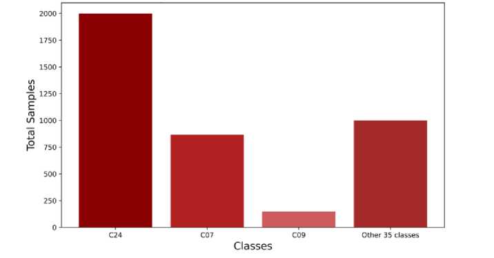
Fig.1. Samples in each class.
-
3.1.1 Single Type
-
3.1.2 Mixed Type
-
3.1.3 Two Mixed Type
In “Single Type” there are 9 classes or wafer images which can be found in Fig 2. Here C1 class is the Normal type which has no defect. From class C2 to class C9 there are 8 basic defect types. All the classes with their corresponding defect pattern name can be seen within Fig 2.
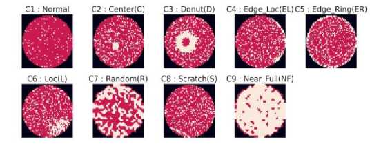
Fig.2. Single Type classes.
“Mixed Type” is created when those 8 basic types of defects are mixed within a single wafer.
This division contains classes of wafers that have mixing of two single defect types which can be seen in Fig 3. From C10 to C22 there are 13 classes in this division. In Fig 3 short forms of each defect type that made into the corresponding wafer are also given at the top of each class image. For example, C12 class has both Center and Loc in the wafer so it is denoted as C12: C+L.
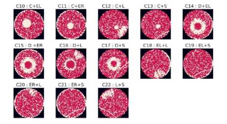
Fig 3. Two Mixed Type classes.
-
3.1.4 Three Mixed Type
-
3.1.5 Four Mixed Type
This division consists of images having three single type defects can be seen in Fig 4. It has a total 12 classes from class C23 to class C34.
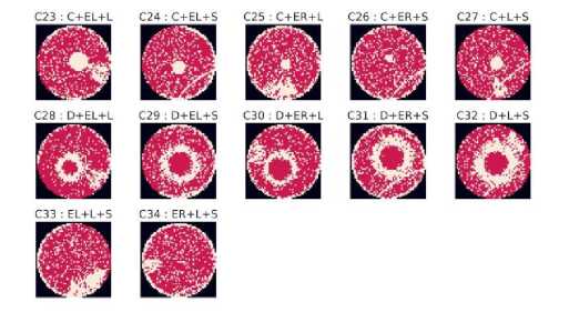
Fig.4. Three Mixed Type classes.
As the name suggests this division contains classes that have four single defects each in Fig 5. There are only four classes there, which are C35, C36, C37 and C38.
С35:C+L+EL+S C36:C+L+ER+S C37:D+L+EL+S C38 : D+L+ER+S
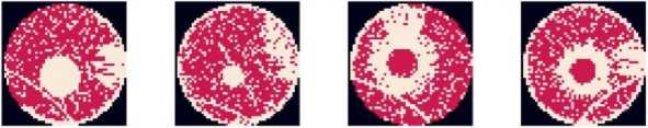
Fig.5. Four Mixed Type classes.
-
3.2. Data Pre-processing
Data preprocessing is one of the most important steps in machine learning and deep learning as the models used in this research are directly affected by the data that is gathered from preprocessing, which controls how much and how easily these models learn. In many cases preprocessing steps need to be different for different models because they require different types of preprocessing. In case of this research as researchers used 4 transformer models these data were preprocessed according to the corresponding model’s demand. At first all of the images were saved to the folders that were named after their classes of which they belong. In this part the images were also divided in train, validation and test sets. The sample distribution can be found from Table 1 and the proportion of train, validation and test set is around 70:15:15 for each of the classes.
Table 1. Distributions of samples in train, valid and test set
|
Classes |
Total Sample |
Train Set |
Validation Set |
Test Set |
|
C24 |
2000 |
1400 (70%) |
300 (15%) |
300 (15%) |
|
C07 |
866 |
607 (≈70%) |
130 (≈15%) |
129 (≈15%) |
|
C09 |
149 |
105 (≈70%) |
22 (≈15%) |
22 (≈15%) |
|
Rest of the classes (each) |
1000 |
700 (70%) |
150 (15%) |
150 (15%) |
As the models in this research were “pretrained models”, images had to be resized according to the requirements of the model they were fed into.
Table 2. Image size and padding for different models
|
Models |
Image Size |
Padding |
|
Vision Transformer (ViT) |
224x224 |
86 |
|
Swin Transformer |
224x224 |
0 |
|
BERT Image Transformer (BEiT) |
224x224 |
86 |
|
FNet |
52x52 |
0 |
For the vision transformer 86 pixels of padding were added to every side of the image to change the image height and width from 52 to 224 (Table 2). Same steps were followed for the BEiT model also. But for the Swin Transformer we added no padding. Instead, we simply changed the size of the image to 224x224 pixels. Although for FNet image size was kept as it is.
-
3.3. Transformer Models
-
3.3.1 Vision Transformer Model
-
-
3.3.2 Swin Transformer Model
Although in recent years, the Transformer Architecture has been widely used in the field of NLP (Natural Language Processing), its applications in Computer Vision were limited. Convolutional Neural Networks were mostly dominant in Computer Vision [11,13] and architectures involving self-attention were being experimented with natural language understanding and end to end object detection [14, 15]. Vision Transformers were designed with the aim of utilizing the standard Transformer architecture in images. This was achieved by sectioning each image into patches and then feeding the linear embeddings of these patches into the transformer layer. These patches are used in the same manner as the tokens used in NLP.
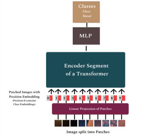
Fig.6. Vision Transformer Architecture.
As Illustrated in Fig 6, the 2D image patches of dimension x E ^ Hxwxc are flattened into dimension xp E ^ wx(p -c) where (H,W) is the image patch resolution, and N = HW(Рг is the number of patches which is also the input sequence length of the Transformer. An embedding is added to this sequence that acts as the image representation. A classification head is attached to this, implemented by a MLP, for both pre-training and fine tuning. Position embeddings are also included in the patch embeddings. The transformer encoder layer used is similar to the ones applied in NLP. Finally, the last layer is a softmax layer that classifies the images. Vision Transformers have low image-centric inductive bias compared to CNNs. This requires Vision Transformers to be trained with large datasets (14M-300M images). These Transformers can then be fine-tuned for a particular application, preferably at higher resolutions [18].
Although conventional Transformer architectures are able to capture long distance dependencies between the pixels of an image, the computational complexity of their self-attention layers have quadratic computational complexity. This makes performing tasks like semantic segmentation difficult.
Swin Transformer addresses this problem by introducing a hierarchical representation in its architecture from the image patches. This is accomplished by performing patch merging operations on neighboring patches as the input moves further into the consequent layers, increasing the overall patch size in each layer. The transformer utilizes a shifted window based self-attention mechanism to link windows from the preceding layers, which results in a significant boost in model representation.
Local windows are placed taking care of the fact that the windows do not overlap each other, and the entire detail of the image is captured. Considering M x M patches per window, the computational complexity on an image of h xw dimensional patches for ordinary MSA (Multi-head Self Attention) W-MSA (window based MSA) are:
O(MSA) = 4hwC 2 + 2(hw) 2 C (1)
П( W - MSA) = 4hwC 2 + 2M 2 (hw)C (2)
Here, there is quadratic complexity with respect to hw in MSA compared to only linear complexity in the W-MSA implementation.
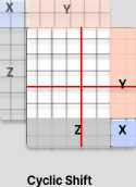
Fig.7. Efficient batch computation using cyclic shift
Multiple Stages are connected one after another and embedding and patch merging operations are performed as depicted in the figure below. The patch merging layer takes a 2 by 2 image layer and concatenates it and then it is down sampled from 4C to 2C. The process repeats in rest of the stages resulting in the expected hierarchical representation [19].
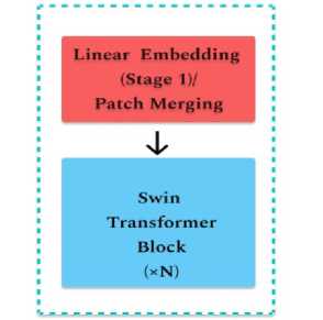
Fig.8. A single Swin Transformer Layer
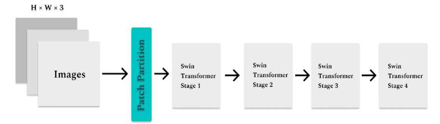
Fig.9. Swin Transformer Architecture
Tokens with a fixed scale are not very appropriate for use in image data training because such activities often include visual objects with a varied range of sizes. And as for detecting the defects in wafer, it can be seen that the size of similar types of defects might vary in great range. This is where the Swin transformer thrives, because of its use of variable patch sizes, by combining shifted windows and patch merging.
-
3.3.3 FNet Transformer Model
Modern Image Transformer models obtain high accuracy in many image-based tasks, such as Image Classification, Semantic Segmentation etc. But these models leave room for improvement in terms of speed and memory consumption. FNet has managed to improve the Transformer in this regard, by utilizing Fourier Transforms in place of the selfattention layer present in conventional Transformers.
FNet achieves comparable accuracies to other Transformer architectures but faster. It achieves 92% and 97% accuracy in GLUE benchmark [16] with respect to BERT-Base and BERT-Large on respectively, training 70% faster in TPUs and 80% faster in GPUs. In terms of longer sequence lengths,
FNet is competitive on the Long-Range Arena benchmark [20] resulting in close accuracy measures to other Transformer architectures but faster.
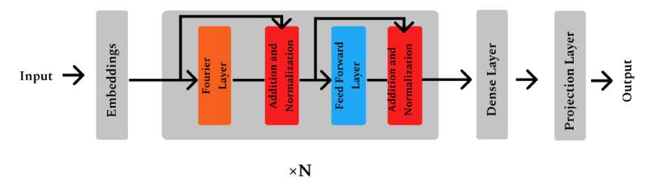
Fig.10. FNet Architecture
Being a self-attention free architecture, FNet leverages a Fourier mixing sublayer followed by a feed-forward sublayer. A 2D DFT is applied by the Fourier sublayer to the Transformer embedding input with dimensions (sequence length Fseq , hidden dimension Fh ).
У = Wsec№(x)))
Here the Fourier Transform can be interpreted as an effective method for token mixing, which provides adequate access to all tokens to the feed-forward sublayers. The alternating encoder blocks can be perceived as applying alternate Fourier and Inverse Fourier operations on the input, switching alternatively from time to frequency domain.

Dividing into patches
Masking random patches applying position embedding
Masked Image Modelling
Applying patch embedding
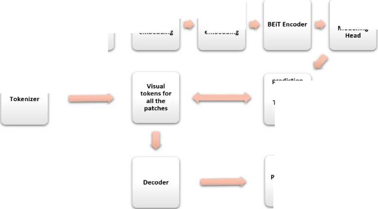
tokens for
Reconstructed Image prediction for the Visual Tokens of masked patches
Fig.11. Working principle of BEiT
3.3.4 BEiT Transformer Model
3.4. Training Configuration
4. Experimental Results and Discussion
This model uses a similar objective function that BERT [21] uses, which is Masked Language Modeling (MLM), which in case of BEiT is Masked Image Modeling or MIM and Next Sentence Prediction (NSP). MLM is used to mask some certain token in a sentence during Natural Language Processing (NLP) training and the model is asked to predict it. In the case of NSP, one single sentence is used as an input and the model predicts what the next sentence will be.
For BEiT [22] images are divided into patches (tokens) and they are masked randomly. After that these patches are flattened into a vector. Then all the embeddings for patches and their positional embeddings are learned and a BERT like architecture is used for these embeddings to pass through. Model predicts the masked image tokens only. All of the image tokens come from image tokenizer. Lastly, the image data is reconstructed using tokens.
Every model was fine-tuned according to their needs in this research. Google Colaboratory Environment was used for this research. As the GPU google provided in the colaboratory has some limitations authors had to use smaller batch sizes which provided better result in the end. Not more than 7 epochs were used in ViT, Swin and BEiT because their validation loss was increasing after that drastically. To complete each model 38 neurons were added at the last layer along with the function “Softmax” and loss “categorical cross entropy”.
In Table 3 we can get a glimpse of what parameter we used for different models in our research.
Table 3. Model Parameters
|
Models |
Epochs |
Batch Size |
Learning Rate |
Patch Size |
|
Vision Transformer (ViT) |
6 |
10 |
0.00001 |
16 |
|
Swin Transformer |
7 |
5 |
0.00001 |
4 |
|
BERT Image Transformer (BEiT) |
5 |
10 |
0.00001 |
16 |
|
FNet |
49 |
32 |
0.001 |
8 |
The precision, recall and f1-score for each defect class was separately obtained while conducting the experiments using the aforementioned architectures. For most classes, the results of the 4 architectures have been found to be near each other, leaving significant changes in only a few defect classes.
As can be seen in Fig 12, In single type wafers, the results are not widely varying in each individual architecture. Overall, the Swin architecture performs the best here and FNet has the lowest precision.
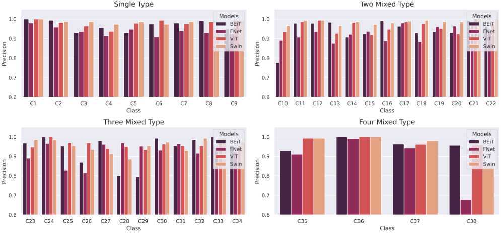
Fig.12. Comparison of Precision (per class) of the 4 Transformer architectures (Swin, ViT, BEiT, FNet)
Swin Transformer and ViT show similar high precision results in detecting Two Mixed Type defects. Here the precision of BEiT drops significantly for the C10 class. Noticeable decline in precision is found in Three Mixed Type defects in C25 and C26 from FNet and C28 and C29 from BEiT. All the models have great precision in Four Mixed Type defects with only a low precision scored in C38 by FNet.
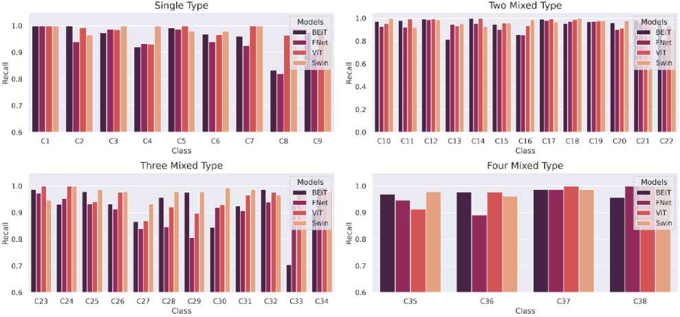
Fig.13. Comparison of Recall (per class) of the 4 Transformer architectures (Swin, ViT, BEiT, FNet)
In terms of recall, in most cases high values are obtained by all 4 architectures. In Single Type defect recall drops noticeably for FNet and BEiT in C8. Recall from BEiT also falls down in C33
in Three Mixed Type architecture. Recall values for Two Mixed Type and Four Mixed Type do not suffer from any major fluctuations.
Lastly, F1-scores obtained also show great results for all 4 architectures. The results only deviate with some significance in C33 falling under Three Mixed Type category, followed by C38 of Four Mixed Type category by BEiT and FNet respectively.
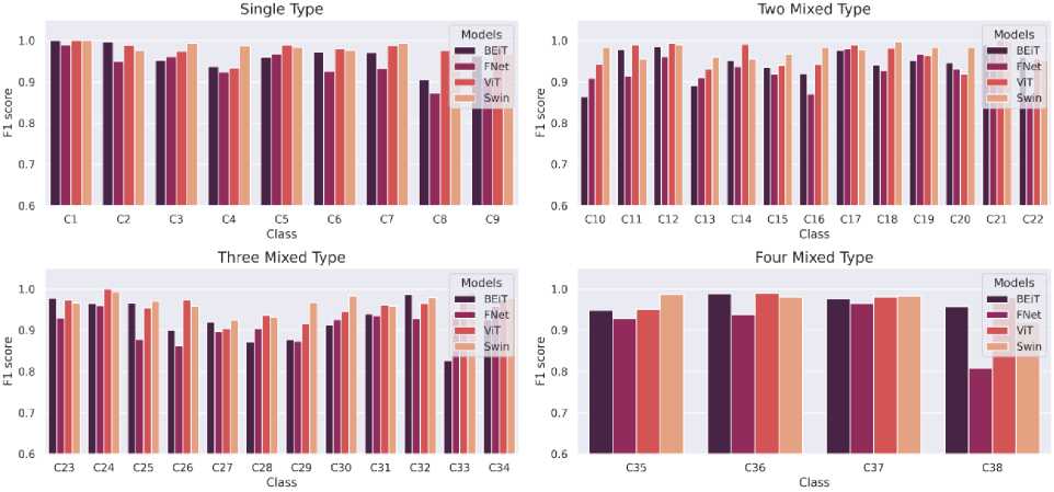
Fig.14. Comparison of F1-Score (per class) of the 4 Transformer architectures (Swin, ViT, BEiT, FNet)
Comparing the 4 methodologies, Swin Transformer model performed better than all of them in this experiment with an accuracy of 97.47% which can be seen in Fig. 15. Only closest to that accuracy is 96.77%, obtained by Vision Transformer (ViT). Remaining two models have accuracy below 95% (BEiT - 94.58%, FNet - 92.86%).
Table 4 presents the performance results of Swin Transformer model that includes Precision, Recall and F1 Score for each class. All the numbers that are in bold font are the one where the Swin Transformer model outperformed other models in this experiment. In case of class C1 this model achieved a perfect 1 score in each section indicating that it accurately distinguished between normal wafers (C1) and defective wafers (C2-C38). Swin also gave better results in many other classes also with different sections. It gave the best result in all sections of class C7 where training samples were a little less than usual. Whereas for class C9 which also had much less training samples this model gave average performance.
Models
Fig.15. Comparison of overall accuracy of the 4 Transformer architectures (Swin, ViT, BEiT, FNet)
Table 4. Performance of Swin Transformer
|
Classes |
Precision |
Recall |
F1 score |
|
C1 |
1 |
1 |
1 |
|
C2 |
0.986395 |
0.966667 |
0.976431 |
|
C3 |
0.986842 |
1 |
0.993377 |
|
C4 |
0.974026 |
1 |
0.986842 |
|
C5 |
0.986577 |
0.98 |
0.983278 |
|
C6 |
0.97351 |
0.98 |
0.976744 |
|
C7 |
0.986842 |
1 |
0.993377 |
|
C8 |
0.943038 |
0.993333 |
0.967532 |
|
C9 |
0.992958 |
0.94 |
0.965753 |
|
C10 |
0.967742 |
1 |
0.983607 |
|
C11 |
0.992806 |
0.92 |
0.955017 |
|
C12 |
0.993289 |
0.986667 |
0.989967 |
|
C13 |
0.966216 |
0.953333 |
0.959732 |
|
C14 |
0.985816 |
0.926667 |
0.955326 |
|
C15 |
0.972973 |
0.96 |
0.966443 |
|
C16 |
0.980132 |
0.986667 |
0.983389 |
|
C17 |
0.989761 |
0.966667 |
0.978078 |
|
C18 |
0.993377 |
1 |
0.996678 |
|
C19 |
0.986577 |
0.98 |
0.983278 |
|
C20 |
0.986577 |
0.98 |
0.983278 |
|
C21 |
1 |
0.993333 |
0.996656 |
|
C22 |
1 |
0.906667 |
0.951049 |
|
C23 |
0.986111 |
0.946667 |
0.965986 |
|
C24 |
0.986842 |
1 |
0.993377 |
|
C25 |
0.954839 |
0.986667 |
0.970492 |
|
C26 |
0.936306 |
0.98 |
0.957655 |
|
C27 |
0.915033 |
0.933333 |
0.924092 |
|
C28 |
0.885542 |
0.98 |
0.93038 |
|
C29 |
0.954545 |
0.98 |
0.967105 |
|
C30 |
0.973856 |
0.993333 |
0.983498 |
|
C31 |
0.930818 |
0.986667 |
0.957929 |
|
C32 |
0.993151 |
0.966667 |
0.97973 |
|
C33 |
0.993289 |
0.986667 |
0.989967 |
|
C34 |
0.97351 |
0.98 |
0.976744 |
|
C35 |
0.993243 |
0.98 |
0.986577 |
|
C36 |
1 |
0.961832 |
0.980545 |
|
C37 |
0.980132 |
0.986667 |
0.983389 |
|
C38 |
0.851852 |
1 |
0.92 |
|
Average |
0.972487 |
0.975487 |
0.973508 |
5. Conclusion
In this work, a comparison was made between 4 state-of-the-art transformer based architectures for detecting wafer defects of multiple mixed and singular categories. It is observed that all 4 of them perform significantly well in detecting these defects across all categories, with Swin Transformer achieving a marginally higher accuracy. Since Transfer Learning can make Transformer Networks highly effective in these scenarios along with a high degree of accuracy, these models can be easily generalized to other defect identification settings and can be trained much faster. The high degree of accuracy and recall also significantly reduces the odds of releasing faulty products out in the market, which is vital for the VLSI industry. Since this is an Image based technique, it is also more cost effective compared to methods like Electron Beam Inspection. In order to better identify physical defects and the root cause of the defects, at the die level, a die level classifier with a back-propagation network should be employed. Combining these two techniques thus results in a complete system for semiconductor defect detection. In this study authors only considered a single dataset for both training and evaluation which had only 38015 images.
Future investigations can be centered around the effectiveness of the sparse counterparts of multiple Vision Transformers for material fault identification and diagnosis. Other Wafer Map Datasets in conjunction could be used for increasing both robustness and accuracy of the model.
References High Accuracy Swin Transformers for Image-based Wafer Map Defect Detection
- J. S. Fenner, M. K. Jeong, and J. C. Lu, “Optimal automatic control of multistage production processes,” IEEE Transactions on Semiconductor Manufacturing, vol. 18, no. 1, pp. 94–103, Feb. 2005, doi: 10.1109/TSM.2004.840532.
- S. P. Cunningham, C. J. Spanos, and K. Voros, “Semiconductor Yield Improvement: Results and Best Practices,” 1995.
- S. Khan, M. Naseer, M. Hayat, S. W. Zamir, F. S. Khan, and M. Shah, “Transformers in Vision: A Survey,” Jan. 2021, doi: 10.1145/3505244.
- H. Lee, Y. Kim, and C. O. Kim, “A deep learning model for robust wafer fault monitoring with sensor measurement noise,” IEEE Transactions on Semiconductor Manufacturing, vol. 30, no. 1, pp. 23–31, Feb. 2017, doi: 10.1109/TSM.2016.2628865.
- J. C. Chien, M. T. Wu, and J. der Lee, “Inspection and classification of semiconductor wafer surface defects using CNN deep learning networks,” Applied Sciences (Switzerland), vol. 10, no. 15, Aug. 2020, doi: 10.3390/APP10155340.
- P. C. Shih, C. C. Hsu, and F. C. Tien, “Automatic reclaimed wafer classification using deep learning neural networks,” Symmetry (Basel), vol. 12, no. 5, May 2020, doi: 10.3390/SYM12050705.
- J. Yu, “Enhanced stacked denoising autoencoder-based feature learning for recognition of wafer map defects,” IEEE Transactions on Semiconductor Manufacturing, vol. 32, no. 4, pp. 613–624, Nov. 2019, doi: 10.1109/TSM.2019.2940334.
- S. Kang, “Joint modeling of classification and regression for improving faulty wafer detection in semiconductor manufacturing,” Journal of Intelligent Manufacturing, vol. 31, no. 2, pp. 319–326, Feb. 2020, doi: 10.1007/s10845-018-1447-2.
- Y. Fu, X. Li, and X. Ma, “Deep-learning-based defect evaluation of mono-like cast siliconwafers,” Photonics, vol. 8, no. 10, Oct. 2021, doi: 10.3390/photonics8100426.
- M. Baker Alawieh, D. Boning, and D. Z. Pan, 2020 57th ACM/IEEE Design Automation Conference (DAC). IEEE, 2020.
- D. Ballard et al., “Backpropagation Applied to Handwritten Zip Code Recognition.”
- A. Krizhevsky, I. Sutskever, and G. E. Hinton, “ImageNet Classification with Deep Convolutional Neural Networks.” [Online]. Available: http://code.google.com/p/cuda-convnet/
- K. He, X. Zhang, S. Ren, and J. Sun, “Deep residual learning for image recognition,” in Proceedings of the IEEE Computer Society Conference on Computer Vision and Pattern Recognition, Dec. 2016, vol. 2016-December, pp. 770–778. doi: 10.1109/CVPR.2016.90.
- A. Wang, A. Singh, J. Michael, F. Hill, O. Levy, and S. R. Bowman, “GLUE: A Multi-Task Benchmark and Analysis Platform for Natural Language Understanding,” Apr. 2018, [Online]. Available: http://arxiv.org/abs/1804.07461
- N. Carion, F. Massa, G. Synnaeve, N. Usunier, A. Kirillov, and S. Zagoruyko, “End-to-End Object Detection with Transformers,” May 2020, [Online]. Available: http://arxiv.org/abs/2005.12872
- A. Dosovitskiy et al., “An Image is Worth 16x16 Words: Transformers for Image Recognition at Scale,” Oct. 2020, [Online]. Available: http://arxiv.org/abs/2010.11929
- Z. Liu et al., “Swin Transformer: Hierarchical Vision Transformer using Shifted Windows,” Mar. 2021, [Online]. Available: http://arxiv.org/abs/2103.14030
- Y. Tay, Z. Zhao, D. Bahri, D. Metzler, and D.-C. Juan, “HyperGrid: Efficient Multi-Task Transformers with Grid-wise Decomposable Hyper Projections,” Jul. 2020, [Online]. Available: http://arxiv.org/abs/2007.05891
- J. Devlin, M.-W. Chang, K. Lee, and K. Toutanova, “BERT: Pre-training of Deep Bidirectional Transformers for Language Understanding,” Oct. 2018, [Online]. Available: http://arxiv.org/abs/1810.04805
- H. Bao, L. Dong, and F. Wei, “BEiT: BERT Pre-Training of Image Transformers,” Jun. 2021, [Online]. Available: http://arxiv.org/abs/2106.08254
