Power Optimized Multiplier Using Shannon Based Multiplexing Logic

Author: P.Karunakaran, S.Venkatraman, I.Hameem Shanavas, T.Kapilachander
Journal: International Journal of Intelligent Systems and Applications(IJISA) @ijisa
Article in issue: 6 vol.4, 2012.
Free access
In Digital Image Processing, Median Filter is used to reduce the noise in an image. The median filter considers each pixel in the image and replaces the noisy pixel by the median of the neighbourhood pixels. The median value is calculated by sorting the pixels. Sorting in turn consists of comparator which includes adders and multiplier. Multiplication is a fundamental operation in arithmetic computing systems and is used in many DSP applications such as FIR Filters. The adder circuit is used as a main component in the multiplier circuits. The Carry Save Array (CSA) multiplier is designed by using the proposed adder cell based on multiplexing logic. The proposed adder circuit is designed by using Shannon theorem.The multiplier circuits are schematised and their layouts are generated by using VLSI CAD tools. The proposed adder based multiplier circuits are simulated and results are compared with CPL and other circuit designed using Shannon based adder cell in terms of power and area and the intermediate state involved in the circuit is eliminated.The proposed adder based multiplier circuits are simulated by using 90nm feature size and with various supply voltages. The Shannon full adder circuit based multiplier circuits gives better performance than other published results in terms of power dissipation and area due to less number of transistors used in Shannon adder circuit.
Shannon adder, DSCH, intermediate state, MCIT
Short address: https://sciup.org/15010270
IDR: 15010270
Text of the scientific article Power Optimized Multiplier Using Shannon Based Multiplexing Logic
Published Online June 2012 in MECS
Low power has emerged as a principal theme in today’s electronics industry .The need for low power has caused a major paradigm shift in circuit design. In recent years, power is being given as much importance as area and performance. In applications such as personal computing devices and wireless communications system, average power consumption is a critical design concern. The cost associated with packaging and cooling such device is significantly high. Since core power consumption must be dissipated through the packaging, increasingly expensive packaging and cooling strategies are required. Unless power consumption is dramatically reduced, the resulting heat will limit the feasible packing and performance of VLSI circuits and systems. Consequently, there is a clear financial advantage to reducing the power consumed in high performance systems. Pass-transistor logic is reported as one of the alternative logic that can enhance circuit performance. Since, signal can propagate using both the source and the gate; its high functionality can reduce the number of transistors in terms of multiplexing control input technique. Since, a PTL-based circuit can consist of only one type of MOS transistor therefore, it has a low node capacitance and as a result CPL enables highspeed and low-power circuits. In this paper, Carry Save Array (CSA) multiplier is used for designing multiplier circuit. This multiplier is constructed by using 4 different adder cells namely proposed adders, Shannon, CPL techniques. The CSA multiplier is constructed using AND gates, half adder, and full adder blocks. The half adder is designed using pass transistor logic which utilizes EX-OR and AND gates, which is shown in Fig.1.
The 1-bit multi operand addition can be extended to an n-bit multi operand addition by cascading the CSA operators. The multiplier is schematised by DSCH3
CAD tool and its layout is generated by Microwind 3 VLSI CAD tool. We have analyzed the basic circuits and proposed adder based multiplier circuits in terms of power dissipation and area and observed better performance in our proposed Shannon based multiplexing logic circuit.
-
II. Design method
The power dissipation and area are reduced due to multiplexing method. The MCIT techniques reduce the number transistor than CMOS design techniques.
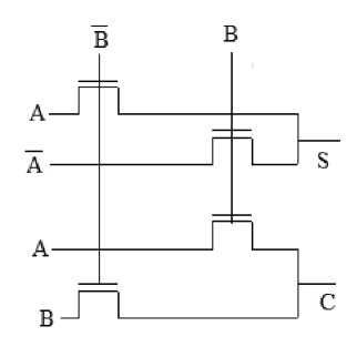
Figure.1 Half adder
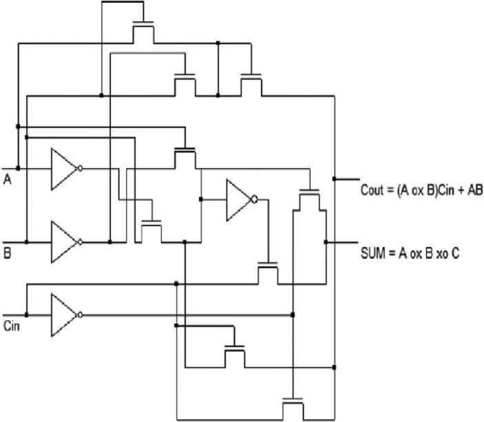
Figure 2.Full Adder
-
III. Proposed Shannon based full adder
The proposed Shannon full adder circuit as shown in Fig.2 combines the multiplexing operation for the sum operation and the Shannon Theorem for the carry operation; the sum and carry circuits are designed based on Standard full adder equations. An input C and its complement are used as the control signal of the sum circuit. The two-input X-OR gate is developed using the multiplexer method. The output node of the two- input multiplexer circuit is the differential node. According to standard full adder equation, the sum circuits need three inputs. In order to avoid increasing the number of transistors due to the addition of a third input, the following arrangement is made, the CPL X-OR gate multiplying with C’s complement input and EX-NOR gate is multiplied with input C, and thereby reducing the number of transistors in the sum circuit. The carry for the half adder is given by,
Half Adder
Carry=A.B
Shannon’s Theorem
Carry= (A.B) + (B.B’)
Full Adder
Sum = A xor B xor C
Sum= ((A xor B).C’) + ((A xor B)’.C)
Carry= (A.B) + (B.C) + (C.A)
Carry= (A+B) C + (A.B)
Existing Adder
Carry= (A+B) C + (A.B) + (B’.C’)
Figure 3. Proposed adder cell
Proposed Adder 1
Sum= ((A xor B).C’) + ((A xor B)’.C)
Carry= (A+B ) C + (A.B) + (B’C’) + (A’.B’)
Proposed Adder 2
Sum= ((A xor B).C’) + ((A xor B)’.C)
Carry= ((A xor B).C) + ((A xor B)’.A)
Table I Truth table of full adder
|
A |
B |
C |
Sum |
Carry |
|
0 |
0 |
0 |
0 |
0 |
|
0 |
0 |
1 |
1 |
0 |
|
0 |
1 |
0 |
1 |
0 |
|
0 |
1 |
1 |
0 |
1 |
|
1 |
0 |
0 |
1 |
0 |
|
1 |
0 |
1 |
0 |
1 |
|
1 |
1 |
0 |
0 |
1 |
|
1 |
1 |
1 |
1 |
1 |
C and C’ node is called the differential node of the circuit. Two complementary ( C and B ) inputs are used in the full adder carry circuit for balancing the circuit and to avoid the floating wire concept. In this circuit, all of the pass inputs are connected at VDD line so that the pass gates are always on. The control input terminals are connected to the function inputs. In the proposed adder 2, from Table I instead of giving all the inputs from external input the internal output from the SUM circuitry acts as input to the carry logic. From the truth table it can be found that when A XOR B output is one, the value of Cout is equals to C. When it is zero, the value of Cout is equals to the value of A. In this circuit, there is comparative reduction in the number of transistors and so reduction in Area and power.
IV.Multiplier design
In this paper, we have designed and analyzed Carry Save Array (CSA) multiplier circuit using our proposed adder cell. The design feature size is 90nm and corresponding supply voltage is 1.2V. The Carry save Array (CSA) multiplier is a linear array multiplier as shown in Fig.3. The linear multiplier propagates data down through the array cell. Each row of CSAs adds one additional partial-product to the partial sum. As the operand size increases, linear arrays grow at a rate equal to the square of the operand size because the number of rows in the array is equal to the length of the multiplier, and the width of each row is equal to the width of multiplicand.
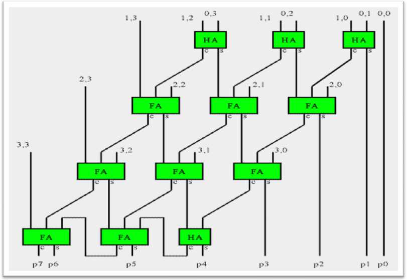
Figure 4. Carry save Array (CSA) Multiplier
V. Results and discussion
In the multiplier array, a full adder with balanced carry and sum delays is desirable because the sum and carry signals are in the critical path. The speed and power of the full adder are very important for large arrays. The 8x8 bit multiplier circuits were simulated with a BSIM4 layout model .We compared the simulated results of our proposed 1-bit adder cell with existing author’s results which shows better performance in terms of power dissipation and area. Our proposed 1-bit adder cell consumes less power, and less area than the various proposed 1-bit adder cells, due to regular arrangement of transistor tree structure, less critical path and multiplexing method of designs. The only drawback of our proposed adder cell is that it occupies larger area. From the simulated results it is clear that the multiplier circuits designed based on the proposed adder cell gives better performance in terms of power, area than the CPL-based adder cell. The main reason for the lower propagation delay of Shannonbased multipliers is that they are balanced in the carry circuits.
Table II shows the results of comparison of various adders with the proposed adders.
Table III shows the results of comparison of multipliers. From the simulated results it is clear that the multiplier circuits designed based on the proposed adder cell gives better performance in terms of power and area than the CPL-based adder cell.
The multiplier circuits imposed parameter analysis, which is done by BSIM 4 analyzer. The total chip of the multipliers is imposed in the temperature analysis. According to Donald A. Neamen v [5], when the temperature increases the total chip leakage current gets decreased.
The total chip leakage current includes the wire current and parasitic components current. The total power dissipation of the multiplier circuit is analyzed by using BSIM 4[10-11]. The total power dissipation of the multiplier circuits is shown in Table III.
TABLE II COMPARISON OF FULL ADDERS
|
Adders |
Area(um2) |
Power dissipation |
Intermediate state |
|
CSL |
97x18 |
37.845uw |
NO |
|
CPL |
30x14 |
0.438mw |
NO |
|
Shannon |
28x13 |
10.644uw |
YES |
|
Proposed Adder 1 |
23x10 |
11.261uw |
NO |
|
Proposed Adder 2 |
14x12 |
7.059uw |
NO |
TABLE III SUMMARY OF RESULTS
|
Adders |
Area(um2) |
Power dissipation |
|
CPL |
317X28 |
0.366mw |
|
Proposed Method 1 |
263x25 |
34.495uw |
|
Proposed Method 2 |
194x24 |
30.243uw |
The Shannon based multiplier circuit gives less power dissipation than other multiplier circuits[12-13].
VI.Application
In Digital Image Processing to find the noise pixel, the median value of the pixel is found. In order to find the median sorting has to be done which is nothing but the comparison of pixels. By employing the proposed adder for compare operation, the median value can be found out with less area and power dissipation.
The individual blocks are the sorter block which includes comparator which is the combination of adders and the multiplexer. The block diagram to find the median of the pixels is shown in Fig.4.
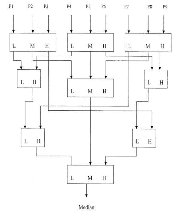
Figure 5. Block diagram of the sorter to find the median
The two pixel sorter and the three pixel sorter are the basic blocks for sorting the nine pixels in order to find the median. They were compared with the proposed adder and the existing adder shown in table IV.
TABLE IV COMPARISON OF SORTER BLOCKS
|
Two pixel sorter |
Three pixel sorter |
|||
|
Adders |
Area (um2) |
Power |
Area (um2) |
Power |
|
CPL |
17.28 |
0.741mW |
99.51 |
1.925mw |
|
Proposed Adder |
82.6 |
26.669uW |
54.34 |
53.426uW |
The sorter which contains proposed adder occupies less area and dissipates less power.
-
VII. Conclusion
The Shannon adder based CSA multipliers circuits are simulated by using Microwind 3 VLSI CAD tools and parameter values are analyzed by using BSIM 4 analyzer. The circuits were compared with existing circuits. Shannon adder based multiplier gives better performance than existing circuits in terms of power dissipation and Area. The proposed multiplier circuits can be used in the low power application of VLSI circuits
-
VIII. Future work
In this paper, power dissipation and area of the multiplier using the proposed adder cell is compared with other multipliers designed using existing adders and used in Digital image Processing. Further it can be used in applications such as FIR filter, FFT, Rank Order Filters where adders and multipliers plays a major role.
References Power Optimized Multiplier Using Shannon Based Multiplexing Logic
- C.Senthilpari, K.Diwakar and Ajay Kumar Singh “Low Power and High Speed 8x8 Bit Multiplier Using Non-clocked Pass Transistor Logics” November 2009
- C.Senthilpari, K.Diwakar and Ajay Kumar Singh “High speed and High Throughput 8x8 Bit Multiplier using a Shannon –based Adder Cell” April 2009.
- Padmanabhan Balasubramanian and Nikos E. Mastorakis “High Speed Gate Level Synchronous Full Adder Designs” WSEAS Transactions on circuits and systems February 2009.
- Z. Abid, H. El-Razouk, D.A. El-Dib “Low power multipliers based on new hybrid full adders” Microelectronics. J (2008), doi: 10.1016/ j.mejo.2008.04.002.
- Donald A. Neamen “Microelectronics: “Circuit Analysis and Design” third international edition, ISBN 007-125443-9, 2007, pp.137-139.
- Zhijun Huang, “High level optimization techniques for low power multiplier design” 2003.
- D. Markovic, B. Nikolic and V.G. Oklobdzija “A general method in synthesis of pass-transistor circuits” Microelectronics Journal31, 2000, pp.991–998.
- Reto Zimmermann and Wolfgang Fichtner “Low-Power Logic Styles: CMOS versus Pass- Transistor Logic” IEEE Journal of Solid-State Circuits, Vol.32, No.7, April 1997, pp.1079–1090.
- C.Senthilpari, K.Diwakar, Ajay Kumar Singh, S.Kavitha, A.Arokiasamy “An Efficient 16-bit Non-Clocked Pass gates Adder Circuit with Improved Power Performance on Power Constraint”.
- K. Navi, M.H Moaiyeri, R. F.Mirzaei, O. Hashemipour, B. M.Nezhad, Jan. (2009), "Two New LowPower Full Adder Based on majority-not Gates" Microelectronics Journal, Elsevier, vol. 40, no. 1, pp. 126-130.
- K. Navi, M. Maeen, O. Hashemipour, , (2009), “An Energy Efficient Full-Adder Cell for Low Voltages”, IEICE Electron. Express, vol. 6, no. 9, pp.553-559.
- J. Lin and Y. Hwang:”A Novel High-Speed and Energy Efficient 10-Transistor Full Adder Design”, IEEE Transactions on Circuits and Systems, Vol. 54, No. 5, May 2007.
- Y. Jiang, A. Al-Sheraidah, Y. Wang, E. Sha, J. Chung, “A novel multiplexer-based low-power fullAdder”.IEEE Transactions on Circuits and Systems-II: Express Briefs. v51 i7.
